Tools: Fusion 360, MODS, EDGB, PCB Milling, Soldering, Arduino
PCB Design with Fusion 360
Unlike two weeks ago, the objective of this week was to use a PCB design tool/software to re-draw a functional circuit such as Niel's echo board. This includes not only milling and soldering components but also PCB design and programming. For this week's assignment, we had to redraw an echo hello-world board and add a button and LED, at a minimum. Additionally, we have to heck the design rules, fabricate it, and test that it can communication
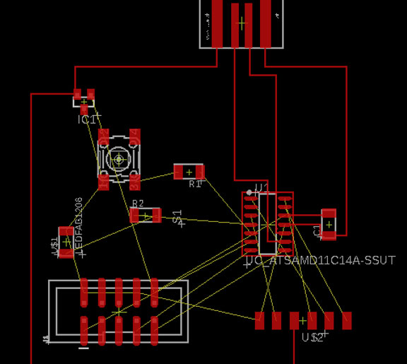
I decided to base the design on Niel's example of the D11C-echo-10 board. This board includes the following components:
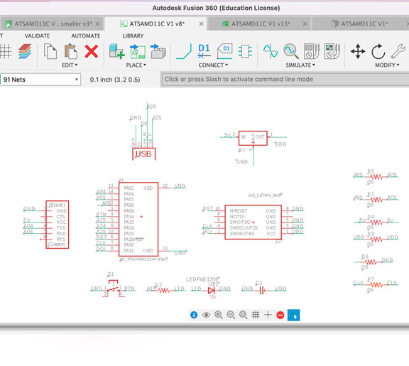
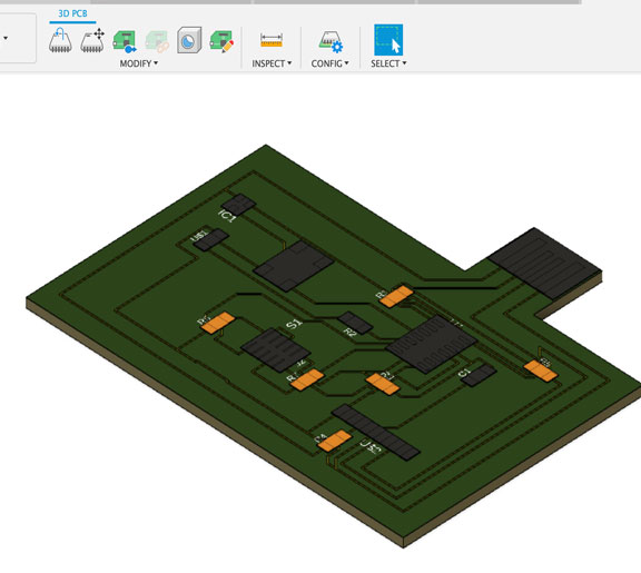
For the design software itself, I used Fusion 360 Electronics Engineer Software from Autodesk and followed Jake's super helpful tutorial. Then, as seen below, I started b adding those components to the board's schematic. After that, I began establishing connections between the pins of the components using the net and name commands. When that was done, I switched to the board view so I could start re-arrange the components and routing the traces. On the right below, you can also see a 3D rendering of the PCB with the 3D view that fusion 360 generates, which is a really nice feature for PCB representation for final projects. In order to have a fully 3D rendered PCB, I would need to load the 3D model of each SMD component which I plan to do next.
Routing Challenge !
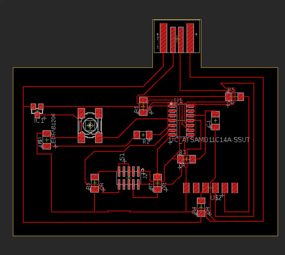
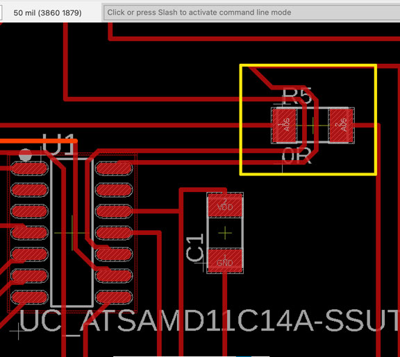
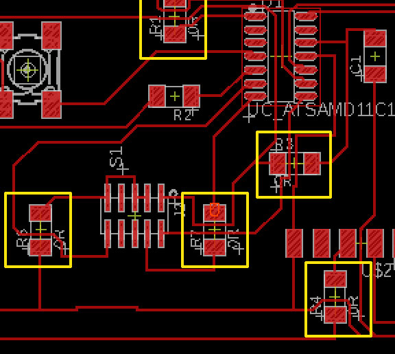
Personally, the most challenging and time-consuming step I experienced during the PCB design process was optimally routing the wires. I tried auto-router many times, but it was not really helpful for me, so I ended up doing it manually. One indicator that I might need to improve my routing skills is that I ended up using five 0-ohm resistors as a trick to jump a wire over another one, highlighted in the yellow boxes below. A better routing strategy would probably yield fewer 0-ohm resistors in the board; I plan to minimize the board in the second version of the design.
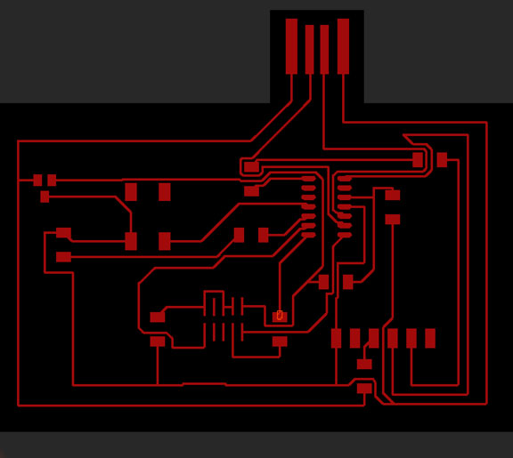
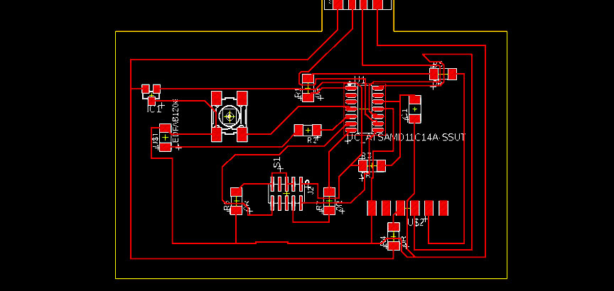
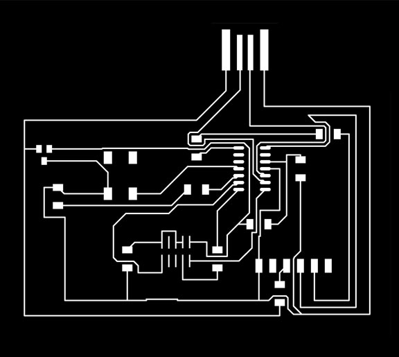
Final PCB Design
The image on the right shows the final top layer layout of the board, showing the traces and pads. I rand drc command to check that Fusion 360 is happy with everything in the design. I set the trae width to be 17 mils to suit the CBA fab milling process. I do think the board is a little large, it can definitely be smaller with a few modifications and removing a few 0-ohm resistors will help.
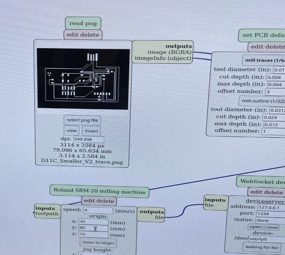
Exporting Design to MODS
Since mods accept PNG files for the board layout and traces files, we need to export PNGs that are appropriate for PCB manufacturing using mods workflow. To do that, I followed these steps: To export a PNG for the traces, I ran these commands
display none to make all of the layers invisible
display top vias pads to display top copper layer only
export image
To export a PNG for the outline, I ran these commands
display none
display bottom dimension vias
export image the same, monochrome, with the same DPI
I modified the exported PNGs in photoshop to ensure enough space at the corners. Below you can find the final monochromatic PNG outline and traces files I loaded into mods in order to start the milling process!

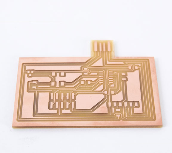
Board Milling !
Similar to our assignment for week 2, here, we used a single-sided copper substarte and the Roland CNC milling machine. For this machine, a 1/64" end mill is used for traces, while a 1/32" end mill is used for cutting the board. After a couple of failures that I will elaborate on in the next section, I was finally able to mill a nice and clean board as seen in the photo
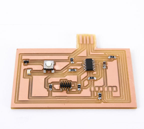
Components Soldering
Next, it was time to stuff the board with the electronic components. I would say that my soldering skill improved from week 2. I did use the microscope and "a lot of flux" in order to facilitate the soldering process, and I was happy with the final result.
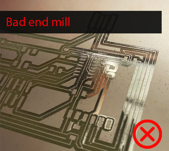
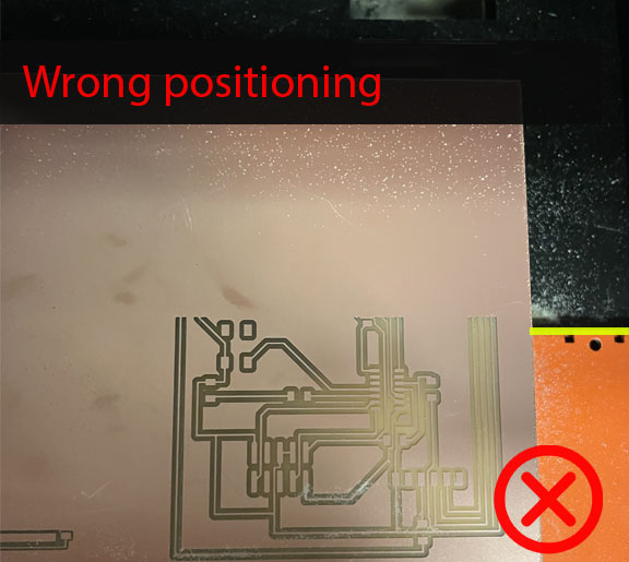
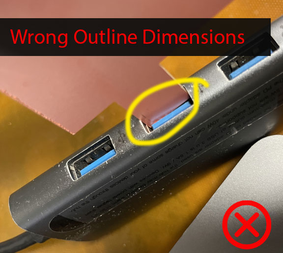
Milling Failures
The milling process this week around was not as smooth as in week 2. Ozgun and I were working together on this and we have saved several failures that I am highlighting below.
Programming the Bootloader
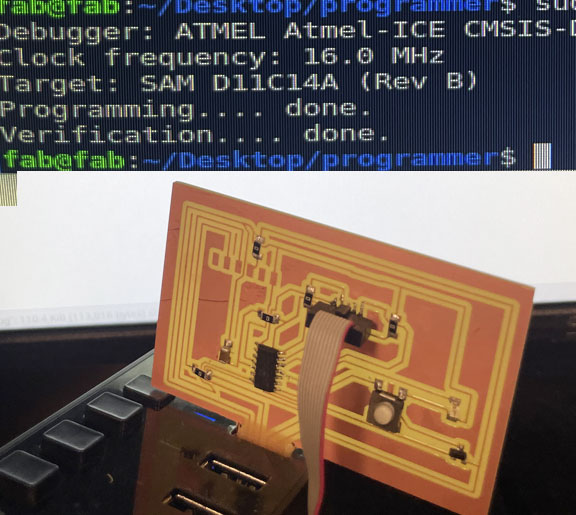
Now that my board is ready, it is time to load the bootloader to be able to use it for various functions later on. I followed Jake's guidein using edbg and downloaded the ATSAMD11C bootloader binary and used the edbg installed in the CBA workshop computer. Upon successful programming, the message on the right should be displayed.
Arduino Setup & Programming
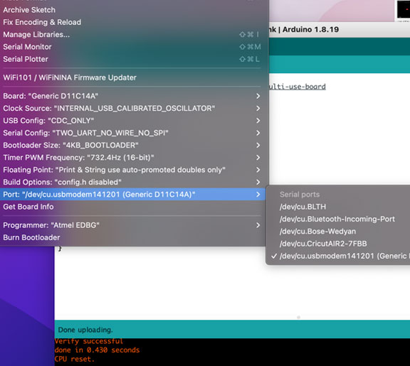
Now that the bootloader is installed, I needed to download and install the Fab SAM core for the Arduino boards library using the library manager in order to get the board recognized by the Arduino. Again, I followed Jake's Fab Arduino SAM guide for this step. After installing it, I could see my device in one of the ports and, after picking the appropriate Arduino board settings for the board I am using. The board is now ready to be used with the Arduino software!!
Push Button and LED Control
As a proof of concept, I programmed the board with two codes of different simple functions. The first code enables the control of the LED using the push button, as seen in the video.
Blinking LED
The second code was the basic blink code, where the LED was programmed to blink continuously as shown in the video
Board testing
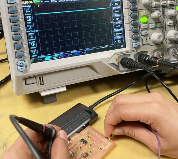
For the group assignment of this week, we had to use test equipment such as the multimeter and oscilloscope in order to check the performance of our freshly made boards and get familiar with these tools. Since Ozgun and I are are quite familiar with using the multimeter, we explored using the oscilloscope this week. Oscilloscopes can give a nice visualization of electrical signals by displaying a plot of voltage vs. time for one or more signals.
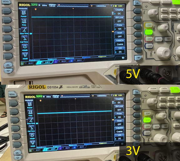
Board testing
We decided to do a simple test where we measured the voltage of two signals we know what value it should be at. For example, when we probed the 5V USB connector trace and GND, we got a value of 5V on the oscilloscope.When we probed the 3V trace coming out of the voltage regulator and GND, we got a value of around 3V on the oscilloscope. !
This was a nice quick test to get familiar with the tool, we plan to explore it more by observing waveforms and frequencies of different signals across the programmed board