week 4: design your own circuit board, and program it!
let's get going on that final project, shall we?
As it stands, my final project is a series of sensors 🡆 that connects to a circuit board 🡆 that talks to a computer. This week and coming weeks that focus on circuit design, embedded programming, and input devices will be good opportunities to get some prototyping/ testing done for my final project.
This week's objective is to design a circuit board (that, at the very least, contains a button and LED) and to make sure it can be programmed and can communicate. I decided to take the chance to design a circuit board that can be used to test the arduino HID library.This library was a recommendation from Neil. Gives your microcontroller the power to act like a keyboard. This is great because Gibber— the live programming environment I plan on using — is built for live keyboard inputs. I will be able to preset some inputs into the hand controller to generate code way faster than it can be typed!
For this week, I will focus on getting the board designed and printed-- this was surprisingly tedious given how straightforward the "program the programmer" week was!
the design
structuring a circuit is harder than it looks...
I wanted the board to have the following features:
- [1] A button tied to an LED to complete this week's minimal assignment
- [2] A button to reset the board
- [3] 2 input buttons that could be programmed using the HID library.
It was recommended that I use the SAMD21E for my circuit board, given its large amount of available ports, storage space, and the fact there was a TA Eagle tutorial available for it. Like in the tutorial, I used Eagle on Fusion 360 to design my circuit board. Eagle splits your design into three files: a schematic file, a PCB design file, and an electronics design file that holds everything together.
All of these files need to be open simultaneously so they can all update at the same time. While this is helpful, shaky wifi connection can cause them to go out of sync :( .
While designing the board, I found it most effective to add 1-2 new items in the schematic file and then move over to the PCB file to position them based on what is already on the board. This really really helped me to remember what was what on the PCB every time I switched over to it. It also helped me figure out when some routing tricks (like routing under a chip or using a 0K resistor as a bridge) had to be implemented.
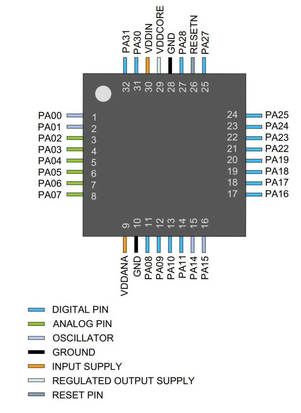
I downloaded the fab library that holds the inventory and sizes of the circuit components in the lab. My previous experiences in classes like 6.115 led me to keep the SAMD21E datasheet close at hand while hooking up ports. While searching for information in this sheet basically doubled my design time, it prevented a lot of microcontroller-frying mistakes. Below is an image of the SAMD21E pinout and power supply information:
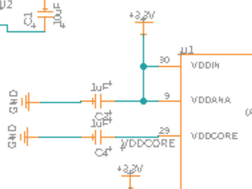
The microcontroller has many available digital pins for use with my buttons, several types of voltage-in ports, and a reset pin. According to the power supply considerations, the VDDIN pin powers I/O lines, VDDANA powers the ADCs, and VDDCORE is for internal voltage regulation. The circuit I am creating has no analog inputs so I tied all reference VDDs (VDDIN, VDDANA) to 3.3V and added bypass capacitors for stability.
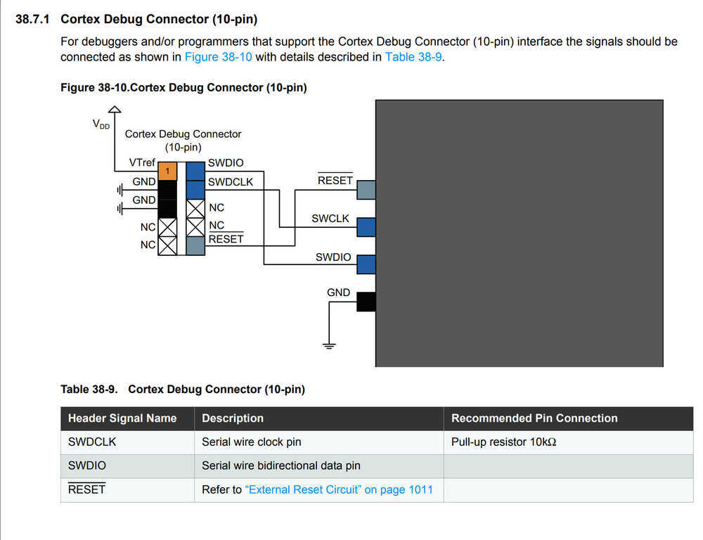
Next, I took a look at connecting a 10 pin connector to the SAMD21E. These pins are what connect the SAMD21E to the programmer for initial flashing. This 10-pin connects to the SAMD21E's reset pin and clock pins. Back to the datasheet! :
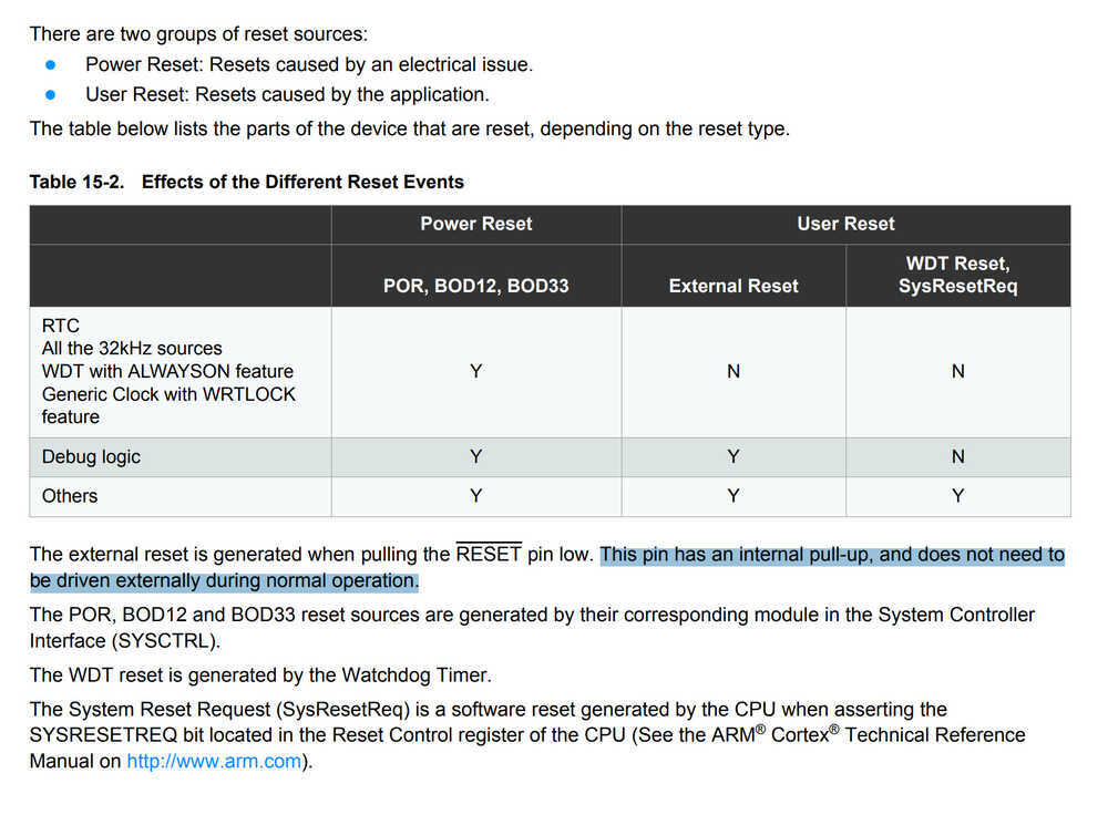
The above datasheet pictures talk about the reset pin and clock pins. In the cortex debug connector diagram, you can see that the reset pin is tied directly to the 10-pin connector's reset pin. This was odd since that point would be floating if the connector pin was not plugged in-- and you don't want a pin like reset randomly activating. I looked into the reset pin settings, as shown in the next image over. The reset pin is active low and has an internal pull-up resistor! This resistor ensures that the reset pin is either high or low-- and not in between. I also added my first button between the reset pin on the connector and SAMD21E. This way, the reset pin would be pulled low only when I pressed the button, completing the circuit that pulls reset to ground. The last image contains information about the serial clock/ data lines. The swdclk needs a 10kOhm pull-up resistor-- I added this to the circuit.
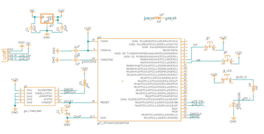
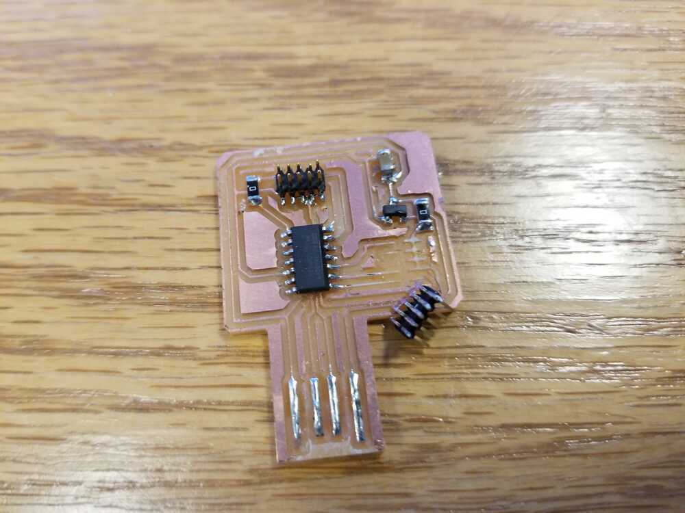
Another fact to consider is that the SAMD21E runs on 3.3V while the USB port (which I want to use for power) runs on 5V. I added a power regulator that converts from 5V to 3.3V to solve this issue. Lastly, I added a button connected to an LED and 2 more buttons connected to digital ports on the SAMD21E.
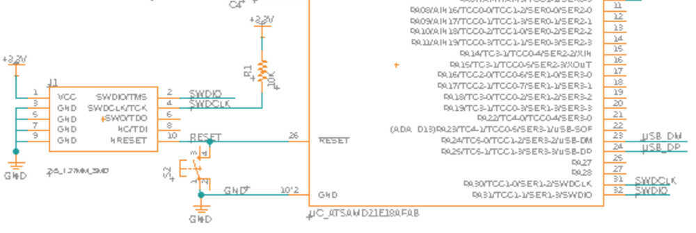
Here's the full circuit again:
Designing a circuit from scratch takes a lot of time, so I will aim to build more general boards in the future to decrease the amount of boards I need to print.
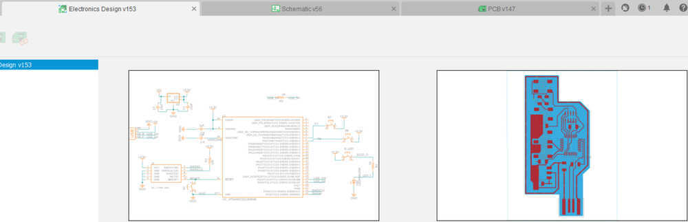

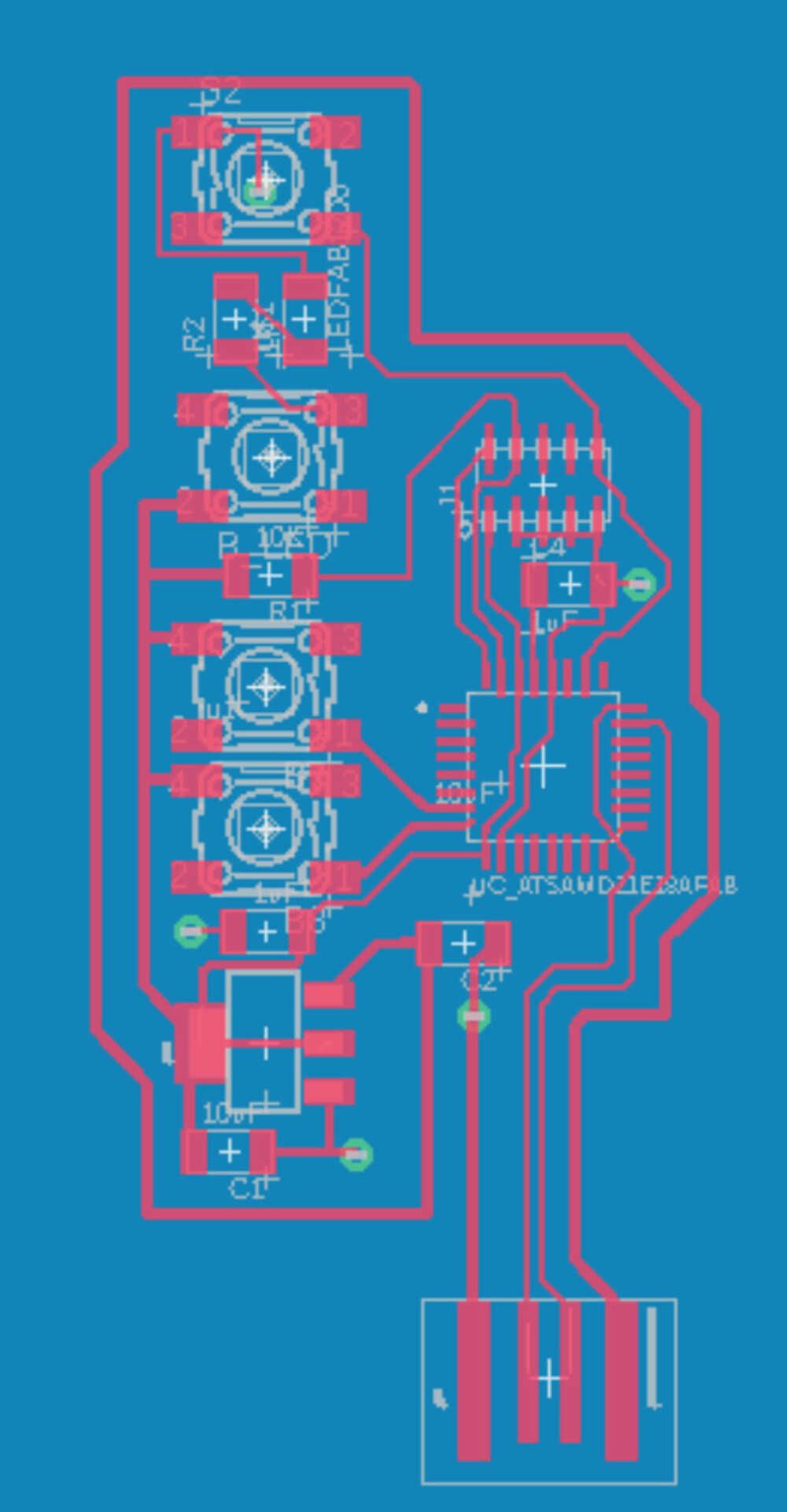
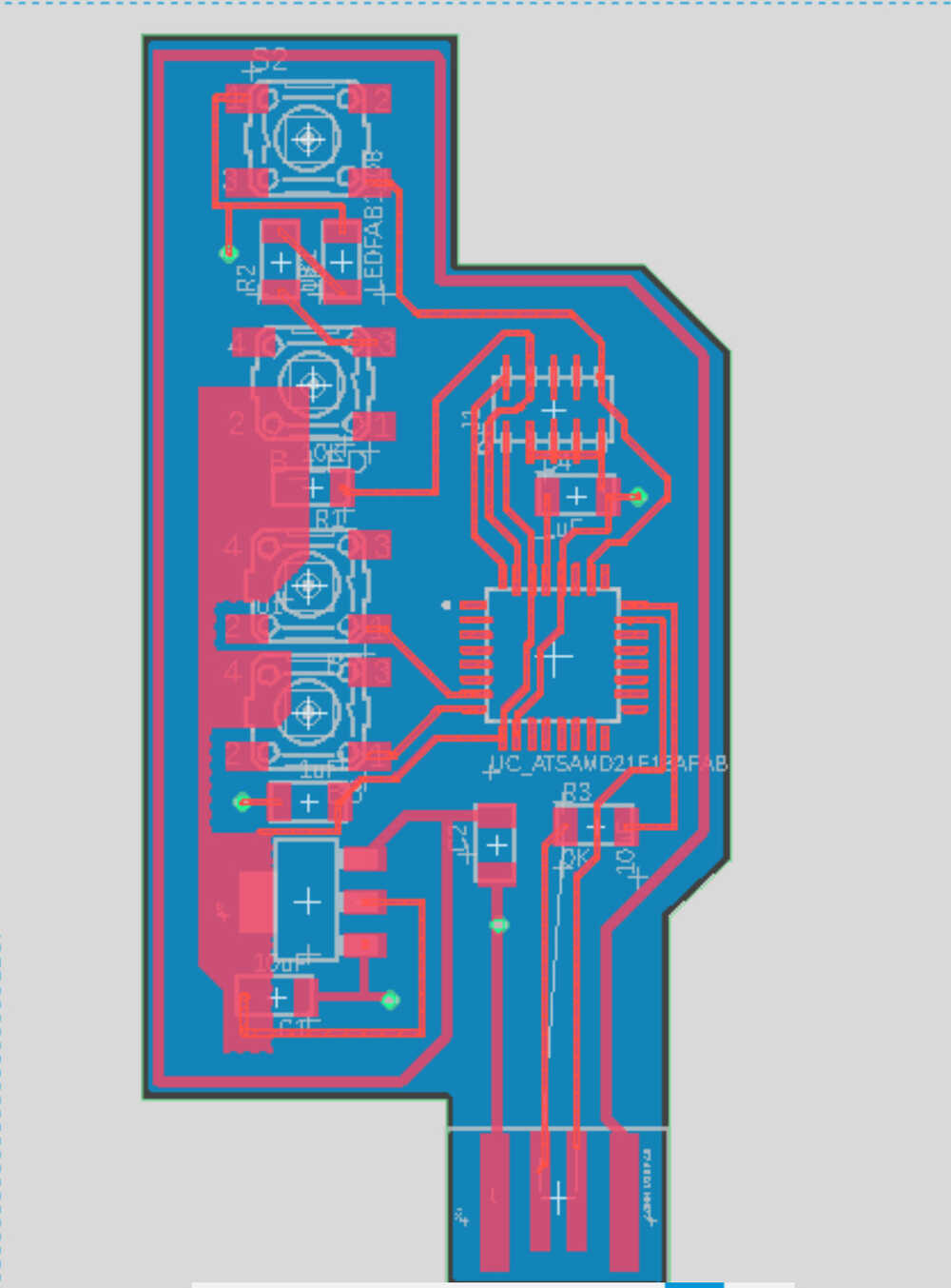
 and the PCB design (the green dots are vias and the blue indicates that there is a bottom copper layer):
soldering and checking connections
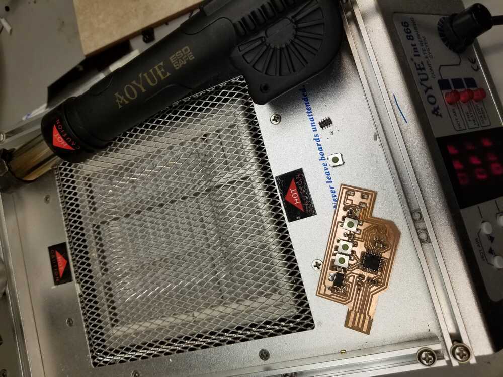
trying not to destroy my newly-milled board
The soldering process is pretty straightforward: read the schematic and solder the components in the correct place. After soldering, use a scope/multimeter to check continuity in the traces. It was helpful to use a microscope to also check between the traces to see if any rogue copper or solder flecks were causing shorts between traces.
- Here are some reminders/notes I took during soldering this week:
-
[1] If your board has vias (holes that tie traces on the top of the board to the copper on the bottom of the board), solder the vias and confirm that the via diameters are correct BEFORE soldering
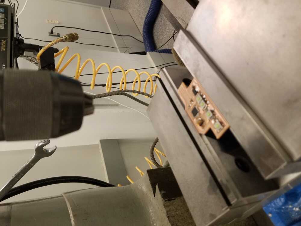
Even after checking and rechecking my via sizes in my design, my vias ended up too small for the little copper tubes you press into them. The issue was a combination of incorrect design rules and incorrect sizing in general. I was not aware of the fact that vias needed these copper tubes so I went ahead and soldered all the components on. This became quite a big problem later since I had to both drill bigger vias and press copper tubes into the board using a press level, all while trying not to destroy the board and its components :/
[2] When removing components from the drawer, check that they are the correct ones... people often misplace things in the lab
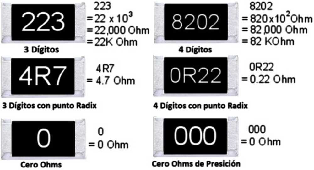
Always double check the component you are soldering on. I could have saved myself the hassle of hot air gun-ing my board to dry to get components to unstick so I could replace them. The first image below shows how to read resistor codes on surface mount resistors and the next image is me using a hot air gun to remove components.
-
[3] Be careful when removing wires from mounted pin connectors. You can rip the trace + the connector off of the board :(
 I was in the process of programming my board using the programmer board I made the previous week. I passed the programmer board to a peer of mine who tried to remove the 10-pin connector wires from the connector and she ended up pulling off the entire connector and the trace it was on.
Luckily this was just the programmer board and not the board I just spent an eternity soldering, drilling, and fixing.
programming
I followed the tutorial from last week, using my programmer (before it broke) to program my board.
I entered the fab lab links into the arduino and wrote a basic program "board_test" to make sure the board could communicate:
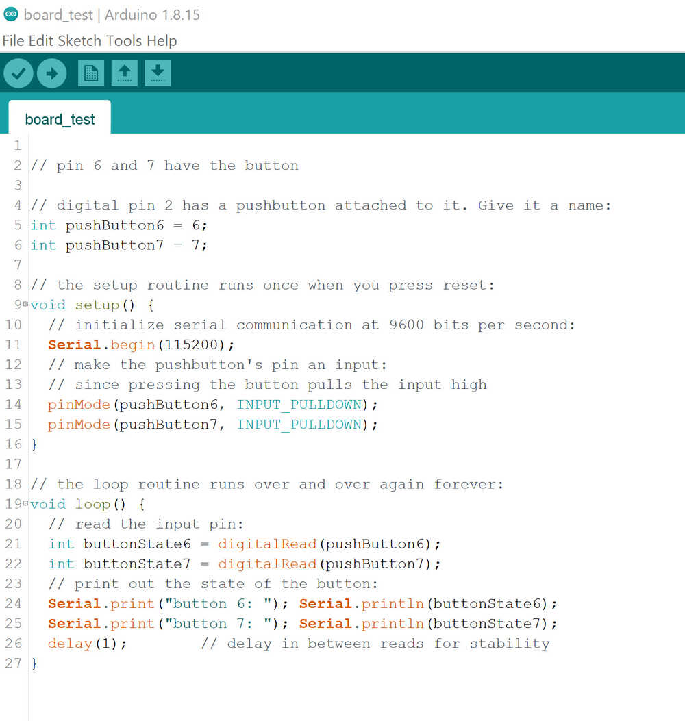
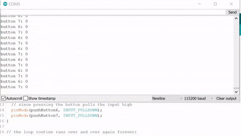
In the test program, I have the 2 buttons printing their value when they are pressed. In the video above on the right, you can see that I press each button individually and then both at the same time.
I initally had some issues with the buttons. Whenever I would touch them, they would activate. It wouldn't matter if they were actually being pressed. I realized after that I had not set the button ports to PULL_UP or PULL_DOWN so the voltage at the port would be floating and my touch would affect it.
I ended up setting the button ports to PULL_DOWN, which is wierd for me since I am used to setting buttons to PULL_UP. I realized that I needed to set the buttons to PULL_DOWN because I had connected the buttons to power. Most of the time, button ports are held at high voltage so buttons can pull them to ground when activated. Actually, when printing the value of the button pin, what I am used to seeing is 1 for unpressed and 0 for pressed. The button function did not change overall, but it was interesting thing to notice. Next time, I'll have the buttons pull pins to ground, since it is probably better for power usage anyway.
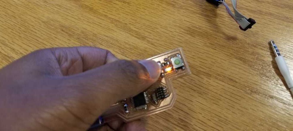
Lastly, here is an image of the LED being turned on by a button press:
 I will use this board to test the HID library in the embedded programs week!