3D Designing, Scanning, and Printing
I designed a circuit board in KiCAD containing a microcontroller with a button and LED connected to it. I then milled out the circuit board on the Othermill in EDS, and uploaded code to it proving it works! Unlike Week 3, I designed and laid out the PCB myself.
PCB Design
Designing the board in KiCAD was surprisingly straightforward. The process starts off with capturing a schematic diagram of the circuit, then drawing that schematic diagram out as a PCB. I’ve previously used Altium, another PCB design software, in my internships, and I found KiCAD to be pretty easy to pick up.
For the schematic, I drew out a microcontroller board similar to the ones on the HTMAA website. It has a JTAG header as usual, but also has a button and LED for added interactivity.
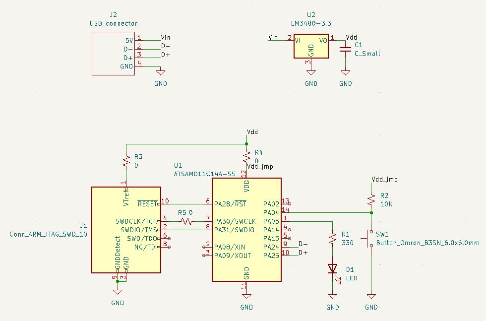
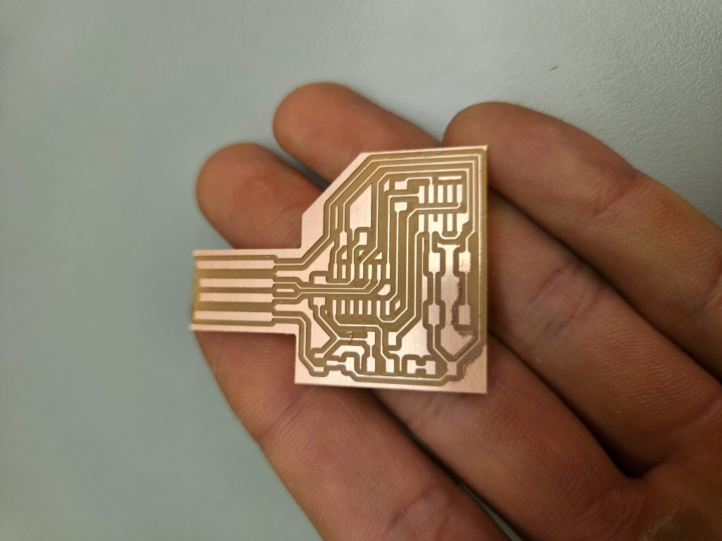
I then copied the schematic over to the KiCAD PCB designer. I started off with all of my components scattered on a blank canvas, with a lot of thin lines indicating which pads connect to which pads. I then arranged the components on the board, drawing wires between each set of pads.
A major design limitation is that the board is a single layer, meaning that all the wires (aka traces) have to be on one side of the board. I cannot, say, route a wire on the bottom side of the board, which would make things a lot easier. This is because we’re using an Othermill milling machine for which making double sided boards is quite hard. Also, the Othermill has a minimum feature size due to its 1/64” endmill, so there needs to be plenty of space between traces.
Largely because of the one-sided constraint, I had to use “jumper” 0-ohm resistors to bridge wires crossing over other wires. I used three zero-ohm resistors in my board to cross over existing traces.
With the board designed, I then exported a set of Gerber files used to fabricate the board. Gerber files are a collection of files, one per layer of the board. In my case there were two Gerber files, one for the traces on the top layer of the board, and one for the outline of the board itself (to know where to cut).
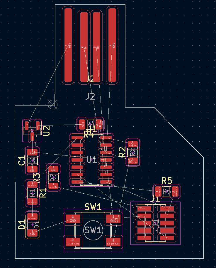
Unrouted board
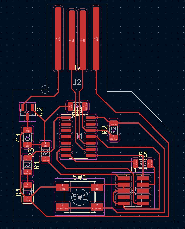
Routed board
PCB Fabrication
We used the Othermill, a purpose-built PCB fabrication mill. The Othermill… mills… the PCB’s using an endmill, specifically a 1/64” or 1/32” endmill. Finer traces get milled first on the smaller endmill, then coarse features and the board overall get milled out afterwards.
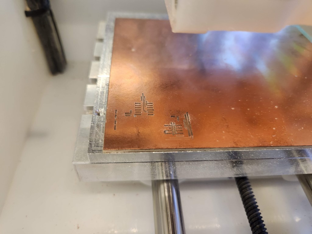
My first attempt, the board wasn’t aligned perfectly, and it was slightly sloped instead of being flat. As a result, the machine milled all of the traces except the ones at the edge of the board. Also the traces came out a bit jagged along the traces, perhaps because the endmill was digging too deep?
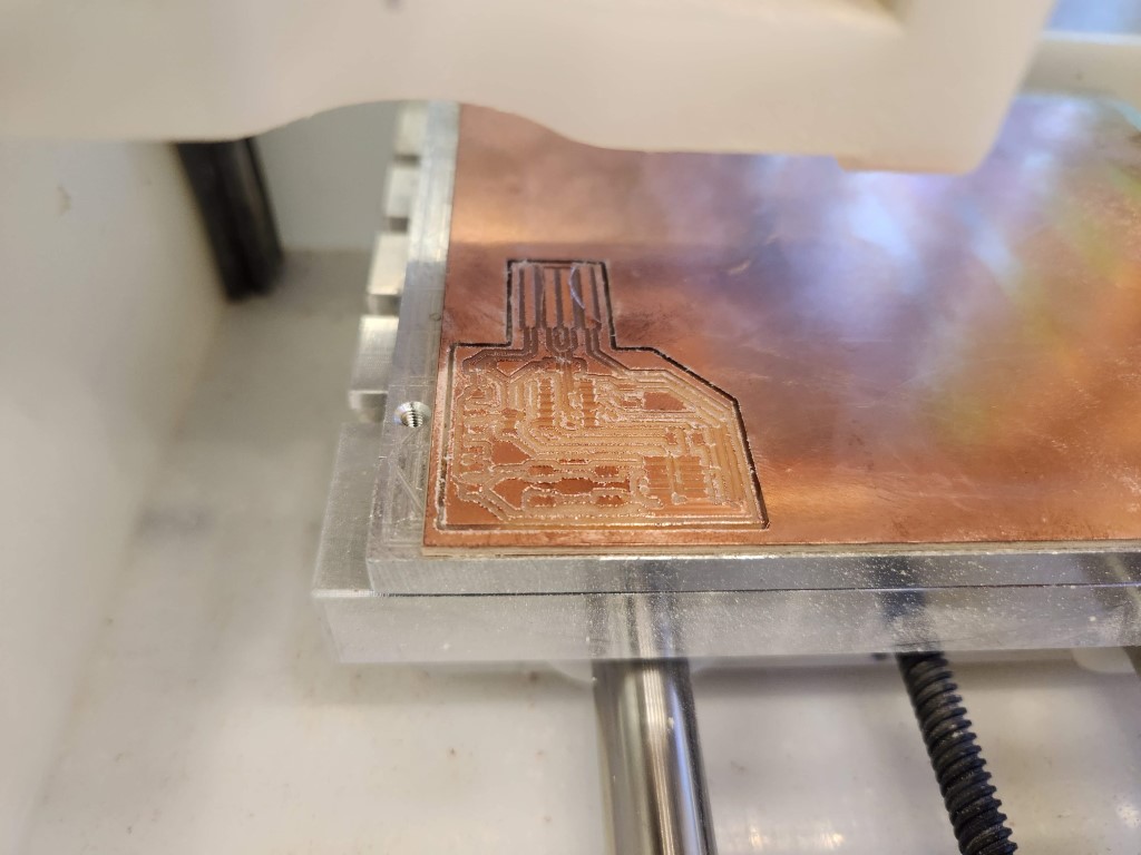
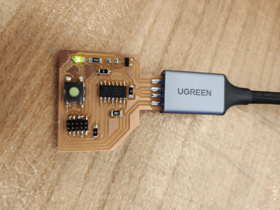
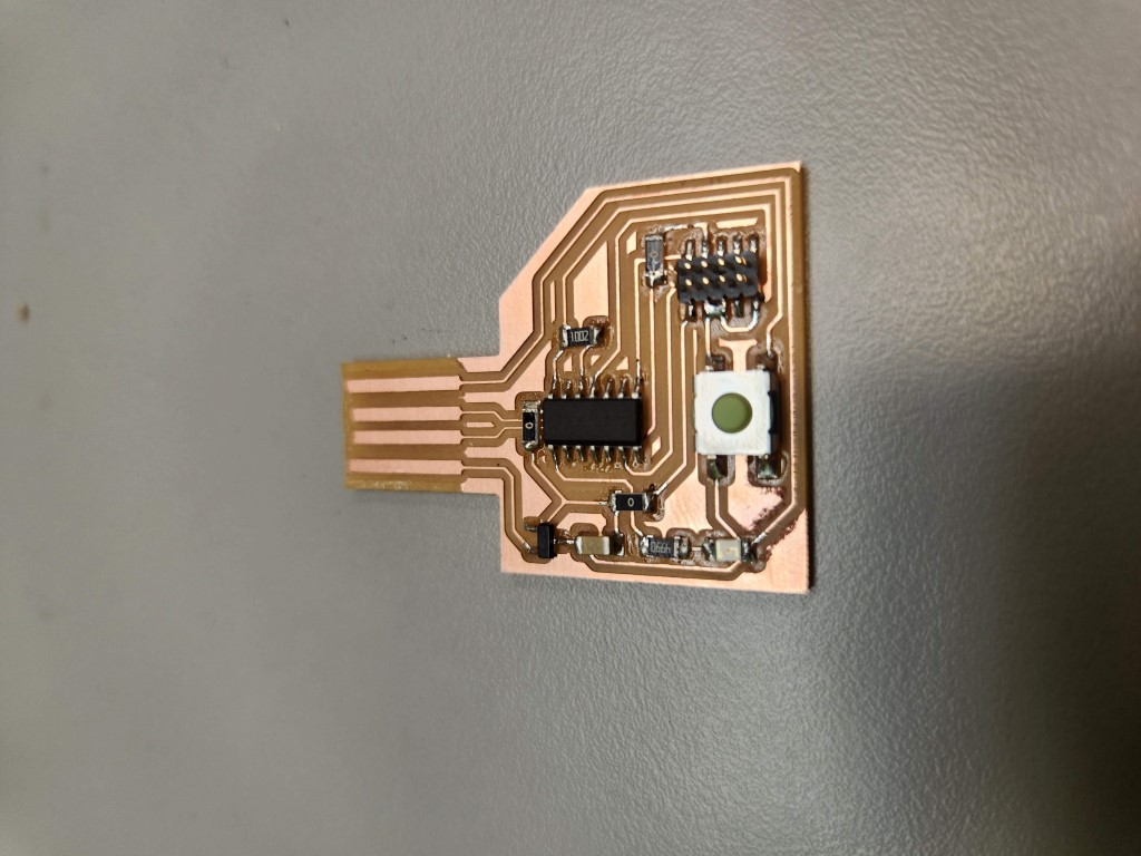
The second time around worked flawlessly. The board came out of the Othermill essentially ready to solder. Soldering went smoothly and took about 30 minutes. I’m getting better with practice, I think!
PCB Programming
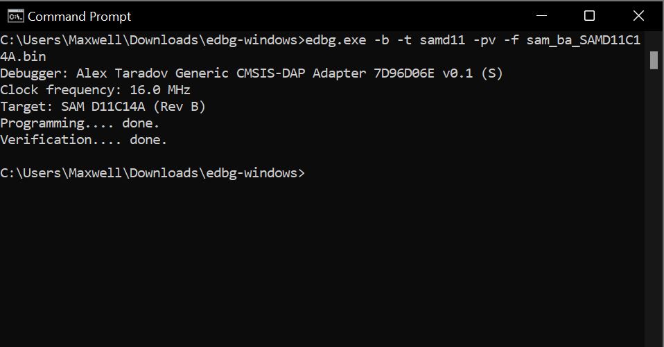
The first step to use the board is to flash a bootloader on it. The bootloader lets the board talk with the Arduino IDE and get programmed more or less like an Arduino. This uses an external JTAG programmer, which I built in Week 2. I hooked up the JTAG IN port of my new board to the JTAG OUT port of the programmer, then connected the programmer to USB. Flashing the board bootloader required downloading EDBG and running:
Then, I set up the Arduino environment for the SAMD11C chip, following these instructions: https://mtm.cba.mit.edu/2021/2021-10_microcontroller-primer/fab-arduino/
I successfully programmed a basic blinking LED driving the onboard LED at pin 5. I also programmed the LED to stay on, then turn off when the button connected to pin 4 is pressed (it’s an open collector switch, so logic is inverted). Both work well!
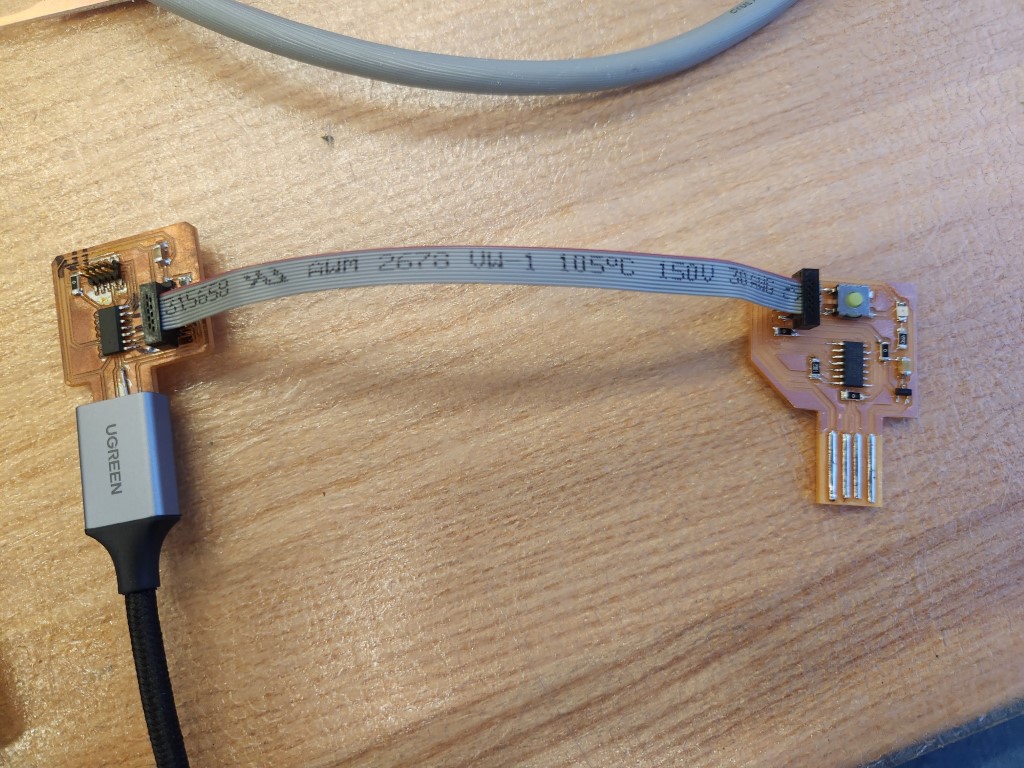
Flashing the board
Blinking light!