05 | Electronics Design
This week’s assignment was to redraw an echo hello world board and add an LED and a button. Before starting I thought that this would be super simple, I’d played around with KiCad over the summer and after messing up numerous times with the electronics production I thought I’d made all the mistakes to make, and it’d be smooth sailing going forwards. I was wrong.
In previous week’s I’d decided upon a project up front and always ran out of time, so this week I took Neil’s advice and began with a spiral. To begin I would just design an echo hello world board. Then once this was done I wanted to great a LED matrix using mutliplexing or charlieplexing (explained below) in the shape of a singer’s head for one of my friend’s birthdays.
Designing the board schematic
During recitation we were showned how Ealge nicely integrates with existing Fusion CAD’s which was enough to get me to abdondon KiCad and commit fully to the Fusion World.
To begin I had to import the FAB component library so that:
- I would only use components EDS had
- I would have accurate footprints
- The FAB components have larger gaps between their pads since we're milling not etching
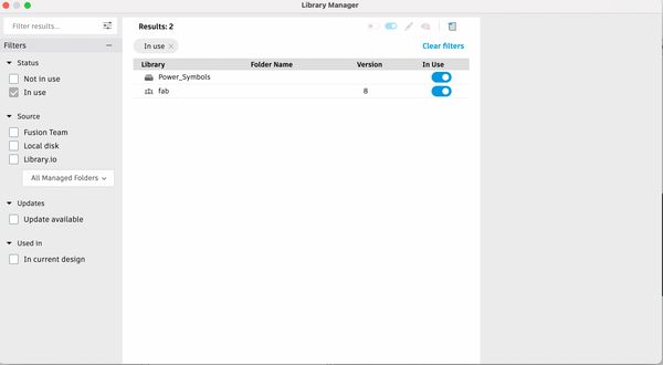
Eagle is a lot slower and jerky than Fusion (maybe there are some settings I need to change) so I also turned off all my other component libraries expect Power Symbols which provide nets for Ground, 5V, etc.
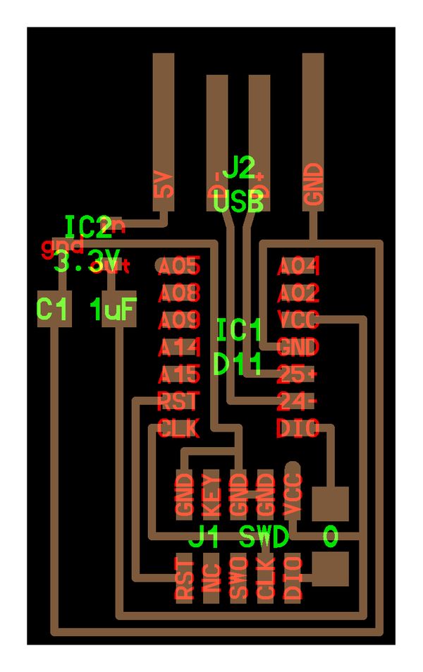
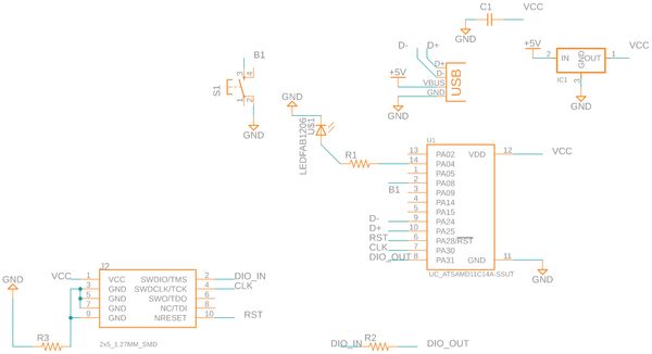
Now I could begin designing the board. First I decided to use the ATSAMD11C chip as it was what I used 2 weeks ago. HTMAA has pictures of what the board should look like so I added all the components to my Eagle schemaic to get ready to net. I had to add another 0 ohm resitor as in the board picture a wire goes under the voltage regulator, however the regulators in EDS were too small to do this with.
At first I was confused with if I added the correct board to my schematic as Eagle had all the pins on the same side. After talking with Anthony I learned that (somewhat annoyingly IMO) the schematic has no relation to a component’s actual footprint. I’m still a little unsure about why there’s such a division between the board itself and it’s schematic.
Once I figured out what was going on, it was time to net. Netting is circuit design’s killer feature. Instead of having to connect each pad together directly, I was able to label parts and Eagle formed a net so that once I switched to the board view they were connected. I use power symbols for the GND and 5V nets and then labeled the pins being used for DIO, CLK, etc.
The base componets were all simple but the LED and button each had a gotcha:
- The LED needs a resistor. I found the part number of the LED in EDS to look up it’s desired amps to figure out what resistor I needed, ~250 ohms.
- To remove noise from the button it needed a pull-up resistor. The button should be default HIGH which is accomplished by connecting the pad we’re reading to a known high voltage, in this case the 3.3v going into the D11C. However, because pullup resistors are so common they’re built into the board so I opted to not add one in Eagle and just turn it on in code.
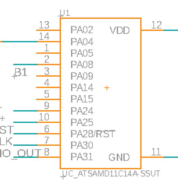
I connected the LED to pin PA04 and the button to PA08. This was a mistake :( If I had looked at the D11C’s schematic I would have seen PA08 is a oscillator pin which can’t be used to do digital reads from. Here’s my (faulty) net:
Routing the board
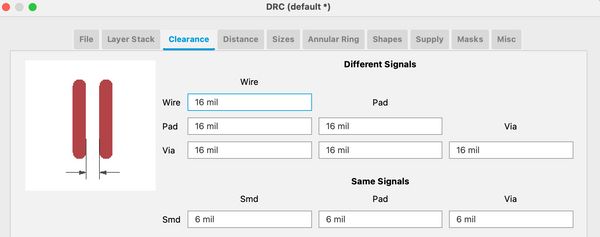
Routing is the second part of circuit design. Once I added all my components and defined the relationships between them, I had to actual plan out where they'd all sit on the board and draw the traces between them.After switching to the PCB from the schematic the first thing I did was define my design rules (Rules > DRC > Clearance) by setting everything to 16mm.
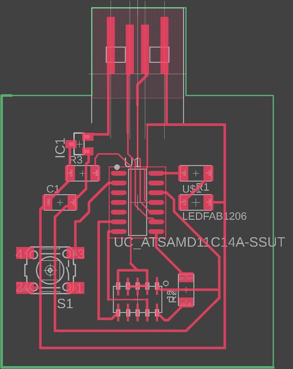
I moved all my components into roughly the positions they were in the provided HTMAA image. Then I used the route tool to connect all of Eagle’s floating white lines. This part was relatively easy but there was a few gotchas:
- For my traces I used two different sizes. The default was 12 but the one’s underneath the D11C needed to be 8 to all fit while complying with the clearance rules. I didn’t change the size at the start and couldn’t figure out how to group change width. Instead I used the command change width [size] and manually clicked the traces to change them.
- The USB component is setup that traces can only leave the pads not enter them. I spent a while wondering why eagle kept doing every shape but a straight line once it got close to the USB.
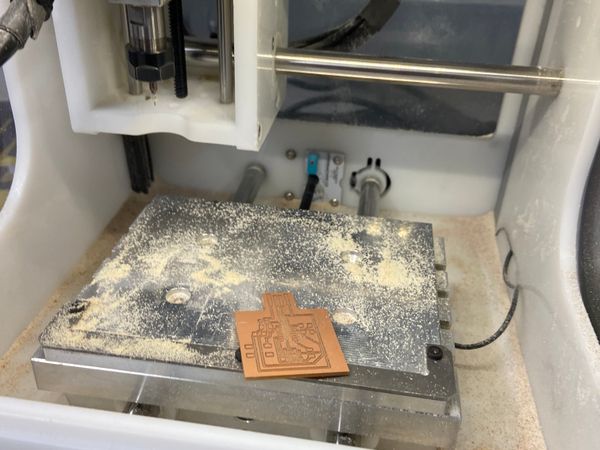
Milling & stuffing the board
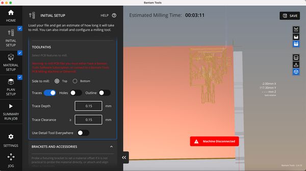
During the electronics production week I used the Roland mill, however in Metropolis (my second home) there are ton of Other Mills which are never used so this week I wanted to finally use how to use them.
After a bit of scratching my head about why nothing was appearing when I googled Batman Othermill I realised that my head read bantman as batman which honestly is a much cooler name :)
This is where everything went wrong, and why I combined these two sections. I had to mill this board 4 times due to things going wrong :(
The Othermill in Metropolis uses the newer Bantman software which was a breeze and I cut my board out easily.
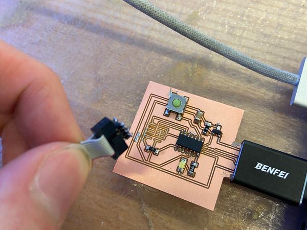
After milling out the board I tried to stuff it, at the start soldering was going much better than with the programmer. However, when I got to the D11C I decied to try out a way I was told about in 2.00b last year were you heat up all the pins at once, apply solder all over them, and the wick up the solder that’s shorting the pads. This did not work. I was left with a mess, and after reflowing, resoldering at least 3 times I gave up on the board and started again.
This time I tried to use the Othermill in EDS however, I didn’t realise that I needed to include both the 1/64” and 1/32” in one job so it told me that the job would take 55m, yikes! I ran over the metropolis and remilled.
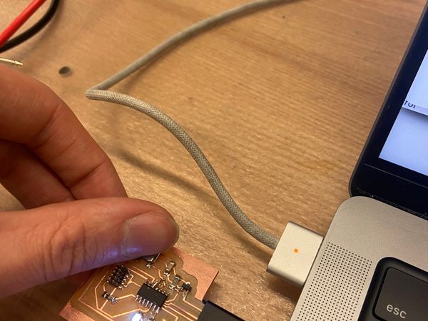
This time, everything soldered perfectly so I went to program the board. I forgot which way the programmer wire went so picked one and plucked it in. When this didn’t worked, I thought ok just switch it around. Too easy! I pulled too hard when removing the wire and pulled off the headers. Bye Bye Board 3
By this time, Anthony was in EDS and told me what I was previously doing wrong with the Othermill, so I was able to mill out another board. Also this time, Anthony told me how to adjust the clearance settings to get the mill to remove the copper around the USB so I didn’t have to do this by hand (it’s necessary to do to avoid shorting the connections).
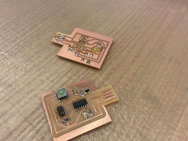
This time everything worked! There were some minor issues with the polarily of the LED and a cold-joint (where the solder is on the component’s pad but not the trace) but once these were fixed by board was soldered, the bootloader was flashed, and I uploaded a simple function!