PCB Fabrication
Table of contents
Group Assignment for PCB Fabrication
Characterize the design rules for your in-house PCB production process.
Extra credit: Send a PCB out to a board house.
As shown in Week 2 of our Group Assignments section, we used the milling machine (Roland SRM 20) to characterize the minimum trace width and clearance that we can mill on the PCB using the linetest.png file.
PCB Milling
I am familiar with PCB fabrication using etching which requires firstly printing the circuit design on a transparent OHP film, then exposing the film to UV light, and finally etching the copper traces using ferric chloride, similar to those steps shown in this instructables.
The milling machine provides a one-time solution to fabricate the PCB. The milling machine uses a high-speed rotating tool to mill the copper traces on the PCB. The milling machine is more suitable for prototyping and small-scale production.
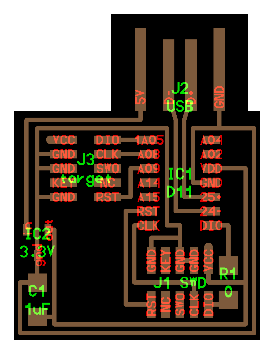
With the guidance and help from Dave, I firstly loaded the desired circuit design (a low-cost JTAG debugger) into the software controlling the milling machine (Roland SRM 20). Then I used the 1/64” end mill, setted the mill parameters accordingly, and calibrated its axial travel distance guided by the GUI to mill the trace of the PCB board. Finally, I switched to the 1/32” end mill with the same setting and calibration steps to mill the clearance of the PCB board.
Here is a screenshot of the milling machine software:

Here are two videos of the milling process: Step 1. PCB Milling Inside (Lines) Timelapse
Step 2. PCB Milling Clearance (Borders) Timelapse
PCB Milling Result
Here is the result of successful PCB milling with clear traces and borders in just one step (compared to the etching process which requires multiple steps and larger failure rate especially consdering the thin copper traces in the circuit design):

Tip from Dave: Sanding the PCB surface to remove edge drill bumps that affect soldering
PCB Soldering
After milling the PCB, I sorted the components required for the circuit design and soldered them on the PCB board. I have some experience with PCB soldering during my undergrad, but this one is particularly challenging because of the small size of the components and the thin copper traces. I got two nice tips from Dave during the soldering process:
- For a component with multiple pins, solder the corner pins to fix the component on the PCB board first, then solder the rest of the pins.
- Use flux to clean the soldering area before soldering, which helps to remove the oxide layer on the copper traces and make the soldering process easier. This is especially helpful for pins with small clearance.
PCB Soldering Result
 PCB with components on it (before soldering) |
 PCB after soldering (under microscope) |
MISTAKE
As you can see from the above pictures, one resistor (0Ω) is missing in the lower side of the PCB, which was pointed out by Anthony and fixed right away at the testing stage. And I made this mistake because I looked into the old board design, which does not include this jump resistor.
Here is the fixed version of the PCB after adding the jump resistor and removing the extra copper traces near the USB connector:

PCB Testing
Following the awesome guide of MTM of using EDBG to program microcontrollers using a cmsis-dap tool, I successfully installed EDBG on my Macbook and tested the PCB board with command:
1
sudo ./edbg -b -t samd11 -pv -f free_dap_d11c_mini.bin
where the test binary file free_dap_d11c_mini.bin is from here.
PCB Testing Result
I just ran a single test and it worked! Here is the screenshot of the PCB test:
 where the last column is the ~160 buck Atmel JTAG debugger and the second last column is our <5 buck JTAG debugger, which does almost the same job. This validates the meaningfulness of this assignment, replacing the expensive JTAG debugger with a much cheaper one.
NOTE
This cost-effectiveness aligns with Dieter Rams’s ideology – Ten principles for good design, where good design is as little design as possible.