# Week 1
**Computer-Aided Cutting**
> Characterize your lasercutter's focus, power, speed, rate, kerf, joint clearance and types.
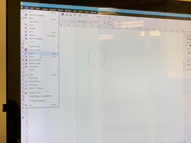
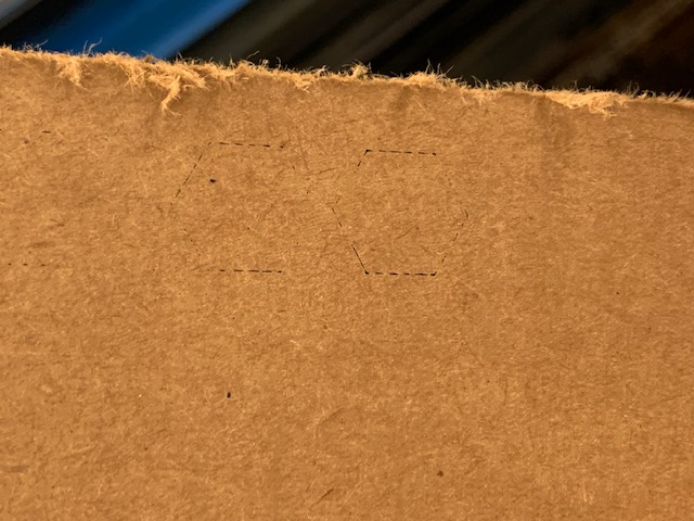
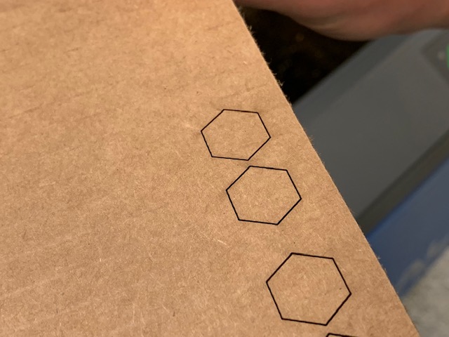
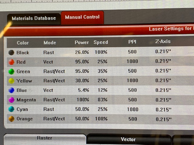
Regarding characterizing the lasercutter. Two hexagons were drawn in Corel and each was set to hairline and a
different color (red and green). These colors were set to vector cut in the print preference window and the speed
and power were varied incrementally (power up and speed down) from the 80% power, 40% speed starting point. The
focus was set with z-axis calibration. The final values that cut all the way through were 95% power and 25% speed,
however, this was later modified to 95% power and 16% speed to ensure the cardboard was cut all the way through. The
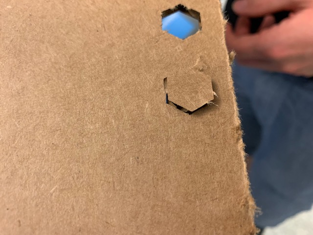
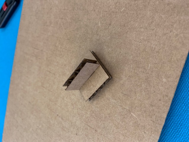
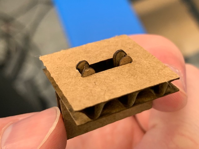
cardboard thickness and kerf were measured with a caliper: 0.17" and 0.004" respectively. A test snap joint was made
with 0.125" thick joint and an overhand of 0.025". This seemed sufficient for a snug joint.
# Week 2
**PCB Fabrication**
> Characterize the design rules for your in-house PCB production process.
> *Extra credit: Send a PCB out to a board house.*
We used the Roland SRM 20 to mill the linetest to characterize the trace widths and clearances that we could mill.
Ideally we would have milled it on the OtherMill since this is what we used to mill our programmer boards, but this
mill only accepts Gerber files and we only had the png file of the linetest (Alec tried to help us convert the png
file to a Gerber file, but to save time we decided to just mill the board on the Roland).
To use the Roland, we opened mods, selected the Roland SRM 20 mill server program and opened our desired png file.
We calculated the tool path using the 1/64" end mill diameter and adjusted the cut depth to ensure that we didn't
cut too deep into the board. After calibrating the machine, we milled the linetest file which can be seen below
compared to the original file.
| [<br />PCB trace width and clearnace testing file](https://academy.cba.mit.edu/classes/electronics_production/linetest.png) | 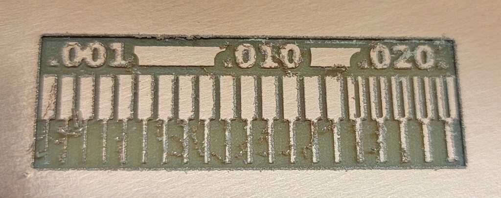<br />Milled PCB using the 1/64" end mill diameter |
| ------------- | ------------- |
Some things we noticed are that the traces down to around 5 mil don't peel. To be safe, it would make sense not to
have traces smaller than 10 mil. Especially since we conducted this test on the Roland which is bigger and more
stable than the OtherMill, meaning that the end mill will vibrate less and thus be less likely to make small
unpredictable movements while milling. Additionally, we noticed that the smallest clearance between traces the mill
could achieve is determined by the diameter of the end mill. We used the 1/64" end mill which is 0.015625". This is
the smallest clearance that this mill can mill. Finally, we observed lots of burring on this board, but we believe
that this is because we milled slightly too deep into the board. This can be remedied by reducing the cut depth.
# Week 3
**3D Scanning and Printing**
> Test the design rules for your 3D printer(s).
We tested the design rules (overhang, clearance with supports; angle, overhang, bridging, wall thickness, dimensions, anisotropy, surface finish, and infill without supports) of the
[Stratasys F120](https://support.stratasys.com/en/printers/fdm-legacy/f120) FDM printer and [Prusa i3](https://www.prusa3d.com/product/original-prusa-i3-mk3s-kit-3/) SLA printer.
The following test pieces were printed on the [Stratasys F120](https://support.stratasys.com/en/printers/fdm-legacy/f120) FDM printer, capable of printing with dissolvable support material.
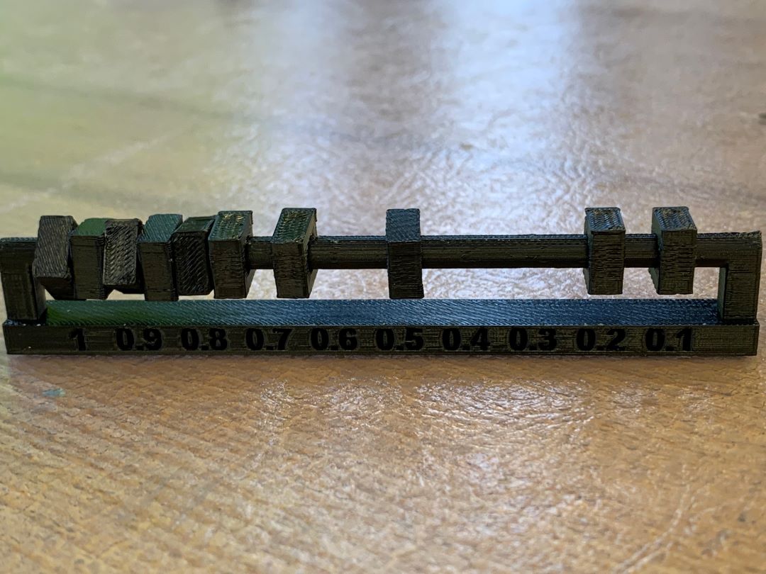
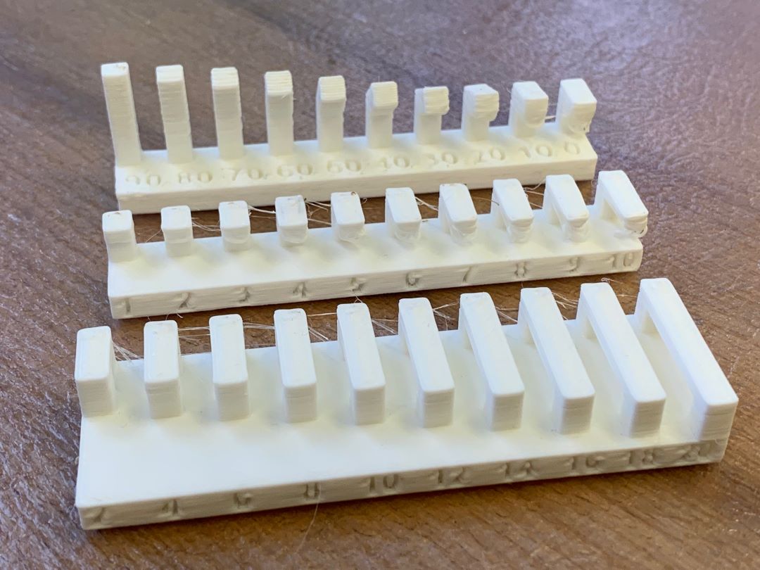
The clearance test below shows how much space must be included between parts for the two parts to slide. With a constant pole thickness, the different sliders had varying inner diameters. All but the last two were able to slide. The 3 from last had considerable friction and was probably at the limit of clearance.
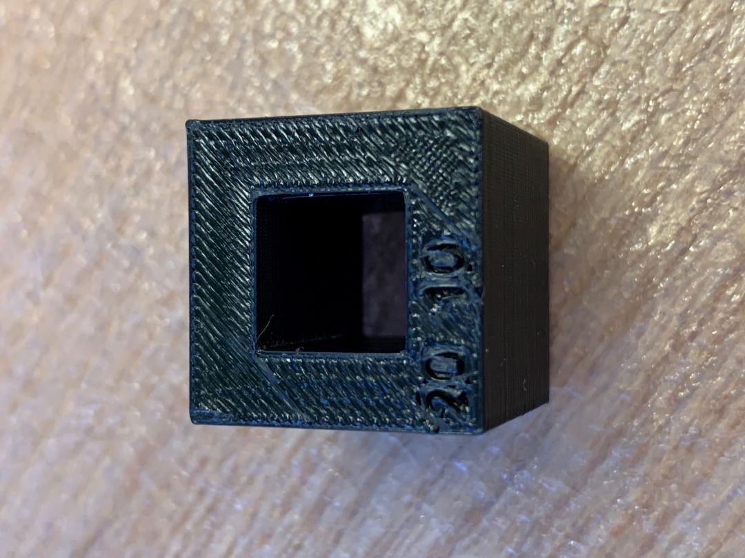
The following box, printed on the Stratasys printer, tests the absolute dimensions that the printer is capable of producing. The outer square nominal dimension is 20 mm and the inner square nominal dimensions is 10 mm. The measured values of the printed piece were 20.168 mm and 9.982 mm, respectively. Tolerances are on the order of 0.2 mm in the xy plane.
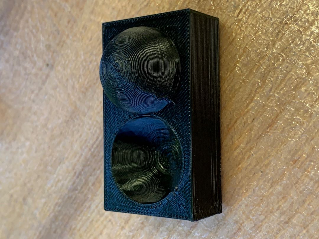
The following part was printed on Stratasys and just demonstrates the differences in surface finish with changing d/dz slope. The step like nature of the FDM produces poor quality finishes with lower d/dz magnitudes due to the finite step size in the z direction during prints.
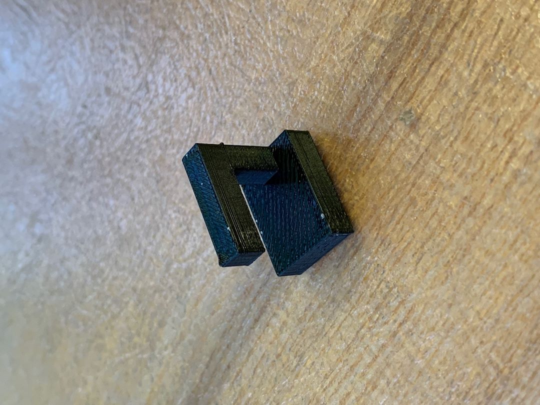
The below part was printed again on the Stratasys to show that a clean cantilevered overhang is possible with proper support material.
The following three parts were produced on the [Prusa i3](https://www.prusa3d.com/product/original-prusa-i3-mk3s-kit-3/) SLA printer to test various overhangs and bridges. From the test, it can be seen that somewhere between 30 and 40 degrees is the minimum angle from the build plane before the print begins to fail. Also, while flat cantilevered structures do not print well at all (just about all failed), a bridge in which the other size is supported does work. This is because the resin is pulled like a strand from one support to the next. This can be done without support material.
# Week 4
**PCB Design**
> Use the test equipment in your lab to observe the operation of a microcontroller circuit board.
To complete this week's assignment we hooked up an ESP32 to an oscilloscope and read its outputs. To make sure the scope leads were on the correct settings, we scoped a known voltage by tying scope ground to ESP32 ground and power to ESP32 5V.
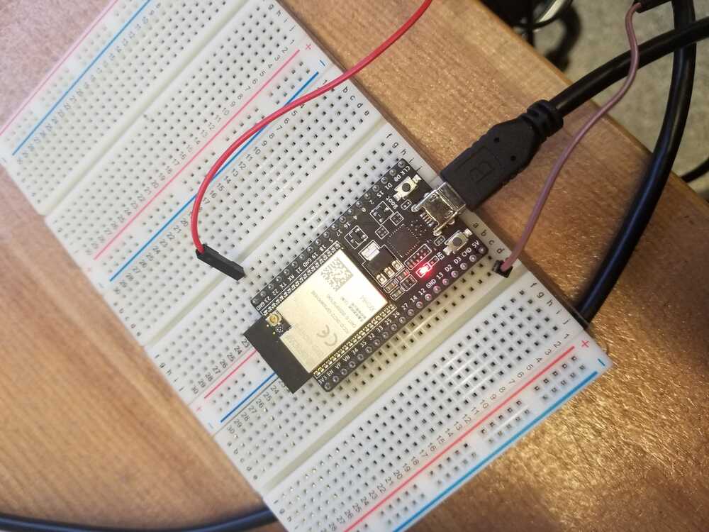
The scope displayed 5V, which matched with the 1X attenuation setting we had on the leads so we were good to test some outputs.
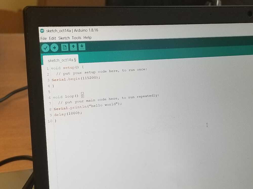
Then, we pulled up a program that printed "hello world" and uploaded it to the board.
We then hooked up the TX (transmit) pin to the scope
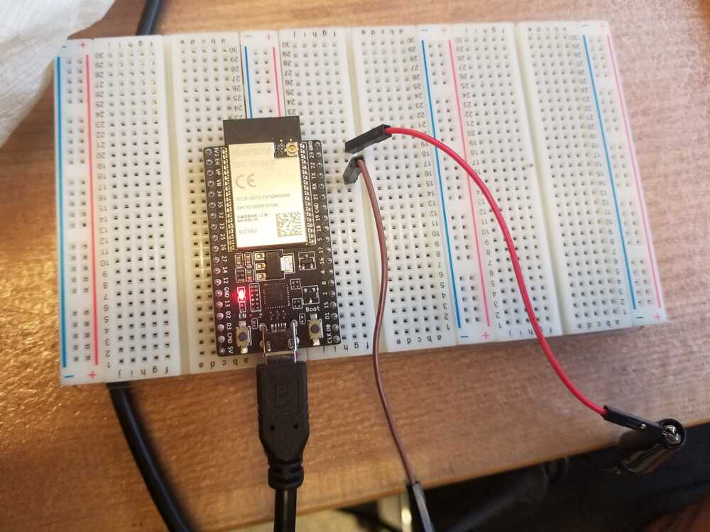
and then read the outputs.
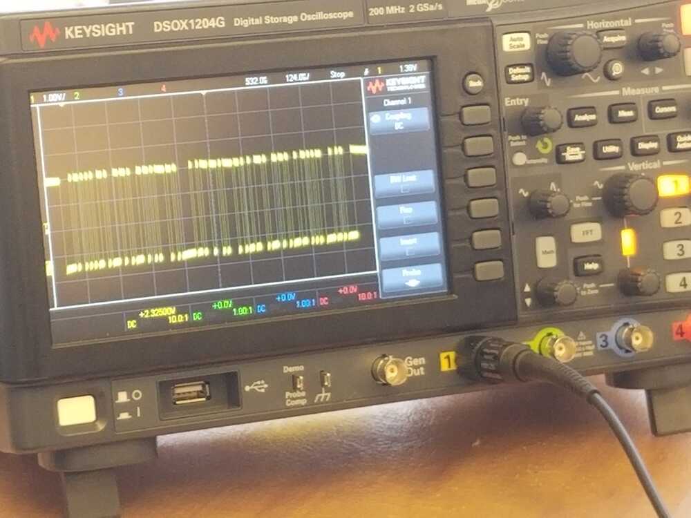
A lot of the output wave was displayed on the screen so we focused a smaller section by using the magnification knob to stretch out the x axis of the wave being read.
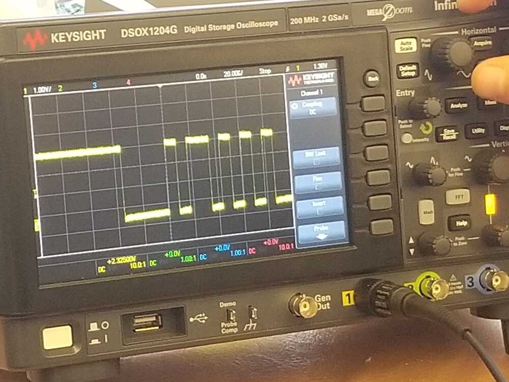
Then, we opened UART settings in the scope and set it to ASCII (which is what the ESP32 should be outputting). When we switched to these setting we got
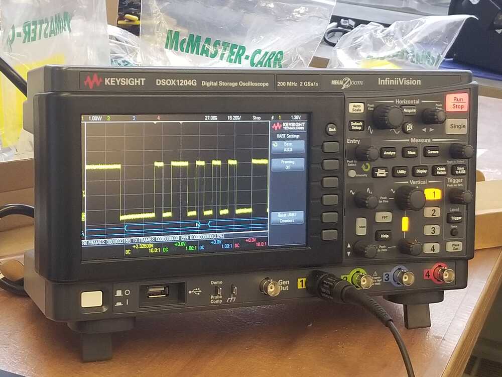
You can see that the ESP32 is indeed printing "hello world"!
# Week 5
**CNC Machining**
> *Do your lab's safety training.*
> Test runout, alignment, fixturing, speeds, feeds, materials, and toolpaths for your machine.
# Week 6
**Embedded Programming**
> Compare the performance and development workflows for other architectures.
# Week 7
**Embedded Programming**
> Review the safety data sheets for each of your molding and casting materials, then make and compare test casts with
each of them.
> *extra credit: Try other molding and casting processes.*
# Week 8
**Input Devices**
> Probe an input device's analog levels and digital signals.
# Week 9
**Output Devices**
> Measure the power consumption of an output device.
# Week 10
**Networking and Communications**
> Send a message between two projects.
# Week 11
**Interface and Application Programming**
> Compare as many tool options as possible.
# [Accessibility](https://accessibility.mit.edu/)
> MIT is committed to providing an environment that is accessible to individuals with disabilities. We invite all to learn
about captioning and accessibility of digital content, and to report any accessibility issues or captioning requests in
the form link on this page.
```url
https://accessibility.mit.edu/
```
#### Note on Math Equations with \\( \LaTeX \\) (using [MathJax 3](https://www.mathjax.org/))
1. Inline equations: only `\\(`/`\\)` works, instead of `$`/`$`. Example: \\(f(x) = \int_{-\infty}^\infty \hat f(\xi)\,e^{2 \pi i \xi x} {\rm d}\xi\\)
LaTeX code:
```latex
\\(f(x) = \int_{-\infty}^\infty \hat f(\xi)\,e^{2 \pi i \xi x} {\rm d}\xi\\)
```
2. Display-mode equations: both `$$`/`$$` and `\\[`/`\\]` works. Linebreaks `\\` in multiline equations needs to be replaced as `\\\\`.
Example:
\\[
\begin{aligned}
\nabla \times \vec{\mathbf{B}} -\, \frac1c\, \frac{\partial\vec{\mathbf{E}}}{\partial t} & =
\frac{4\pi}{c}\vec{\mathbf{j}} \\\\
\nabla \cdot \vec{\mathbf{E}} & = 4 \pi \rho \\\\
\nabla \times \vec{\mathbf{E}}\, +\, \frac1c\, \frac{\partial\vec{\mathbf{B}}}{\partial t} & = \vec{\mathbf{0}} \\\\
\nabla \cdot \vec{\mathbf{B}} & = 0 \end{aligned}
\\]
LaTeX code:
```latex
\\[
\begin{aligned}
\nabla \times \vec{\mathbf{B}} -\, \frac1c\, \frac{\partial\vec{\mathbf{E}}}{\partial t} & =
\frac{4\pi}{c}\vec{\mathbf{j}} \\\\
\nabla \cdot \vec{\mathbf{E}} & = 4 \pi \rho \\\\
\nabla \times \vec{\mathbf{E}}\, +\, \frac1c\, \frac{\partial\vec{\mathbf{B}}}{\partial t} & = \vec{\mathbf{0}} \\\\
\nabla \cdot \vec{\mathbf{B}} & = 0 \end{aligned}
\\]
```
___
<small>&copy; 2022 [HTM(A)A'22](https://fab.cba.mit.edu/classes/MAS.863/) [EECS Section](https://fab.cba.mit.edu/classes/MAS.863/EECS/). Template adapted by [Y. Liu](https://fab.cba.mit.edu/classes/MAS.863/EECS/people/Yang/), powered by [`strapdown.js`](https://ndossougbe.github.io/strapdown/), [Markdown](https://ndossougbe.github.io/strapdown/demos/markdown_syntax.html), and [MathJax 3](https://www.mathjax.org/) for \\(\LaTeX\\) rendering.</small>