This week, I explored electronics design.
In order to use Eagle, I first had to download the fab library so that the footprints would match the components that are stocked in the lab. I used Eagle to design the board from Week 2, but with a LED and switch added. I have no prior experience with Eagle, so it was very hard to learn the UI.
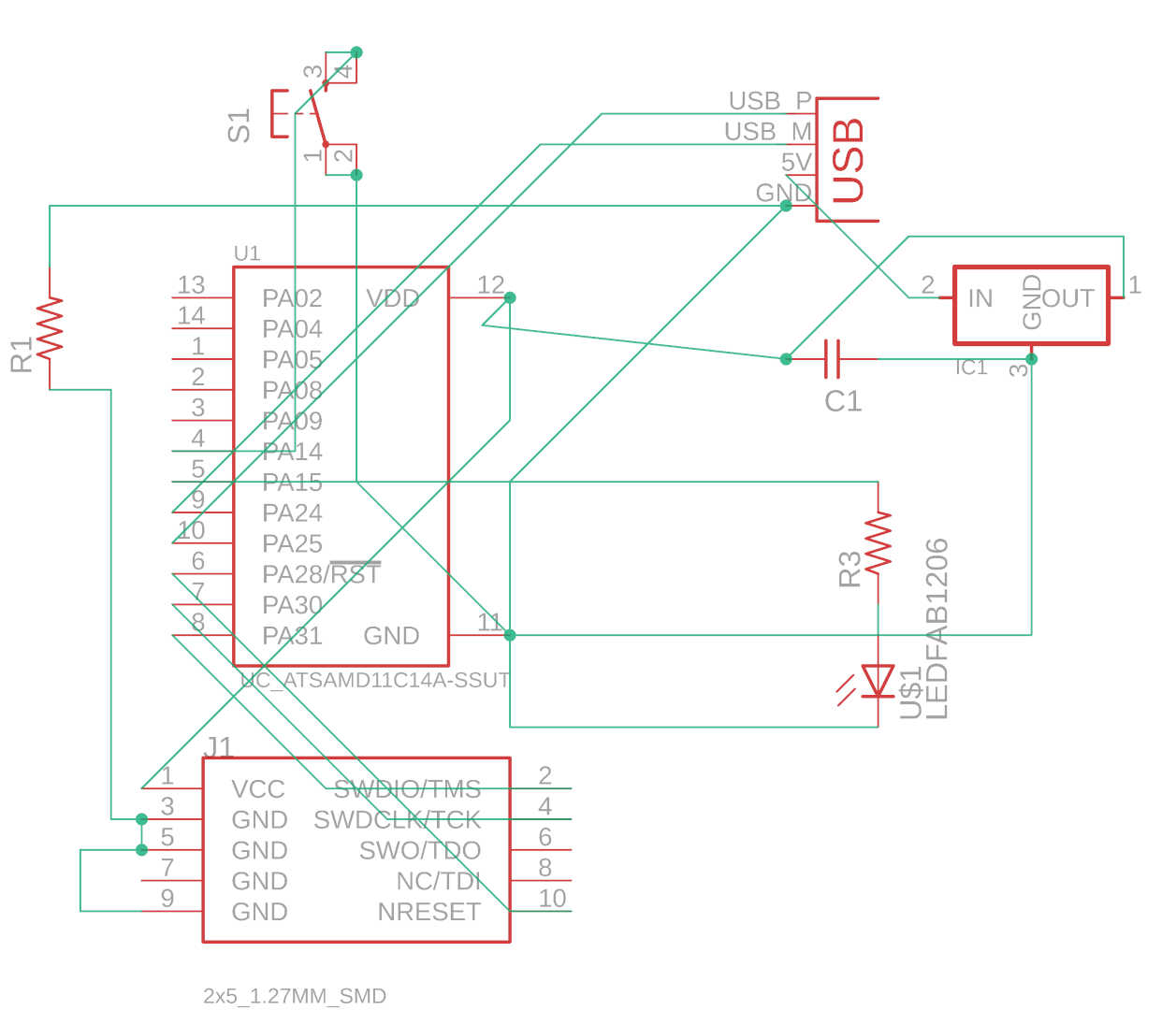
The most frustrating part was routing. Trace width was 8mil (down to 6mil in narrow areas) and clearance was 16mil. Trace width option pops up when placing routes. Clearance can be changed under "RULES" → "DRC". I ended up routing two paths under a single resistor, which was very risky, and using only one jumper (0 ohm resistor). The new board was almost the same size as Week 2's board.
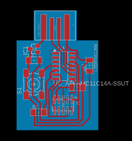
To export the traces and outline as png files, use the command line. Type "display none," and then from the drop down menu, select either "1 Top" for traces or "16 Bottom" for outline. Type "export image" and a window will pop up. Choose 800dpi and monochrome, and pan/zoom so that the board is in the bottom left corner of the window, then do "Area - Window". This ensures that the origin is close to the board.
This process was almost identical to Week 2, and I used the same machine, the Roland SRM20. On the first try, the tape did not fully secure the board when milling the outline, so it was ruined at the very end.
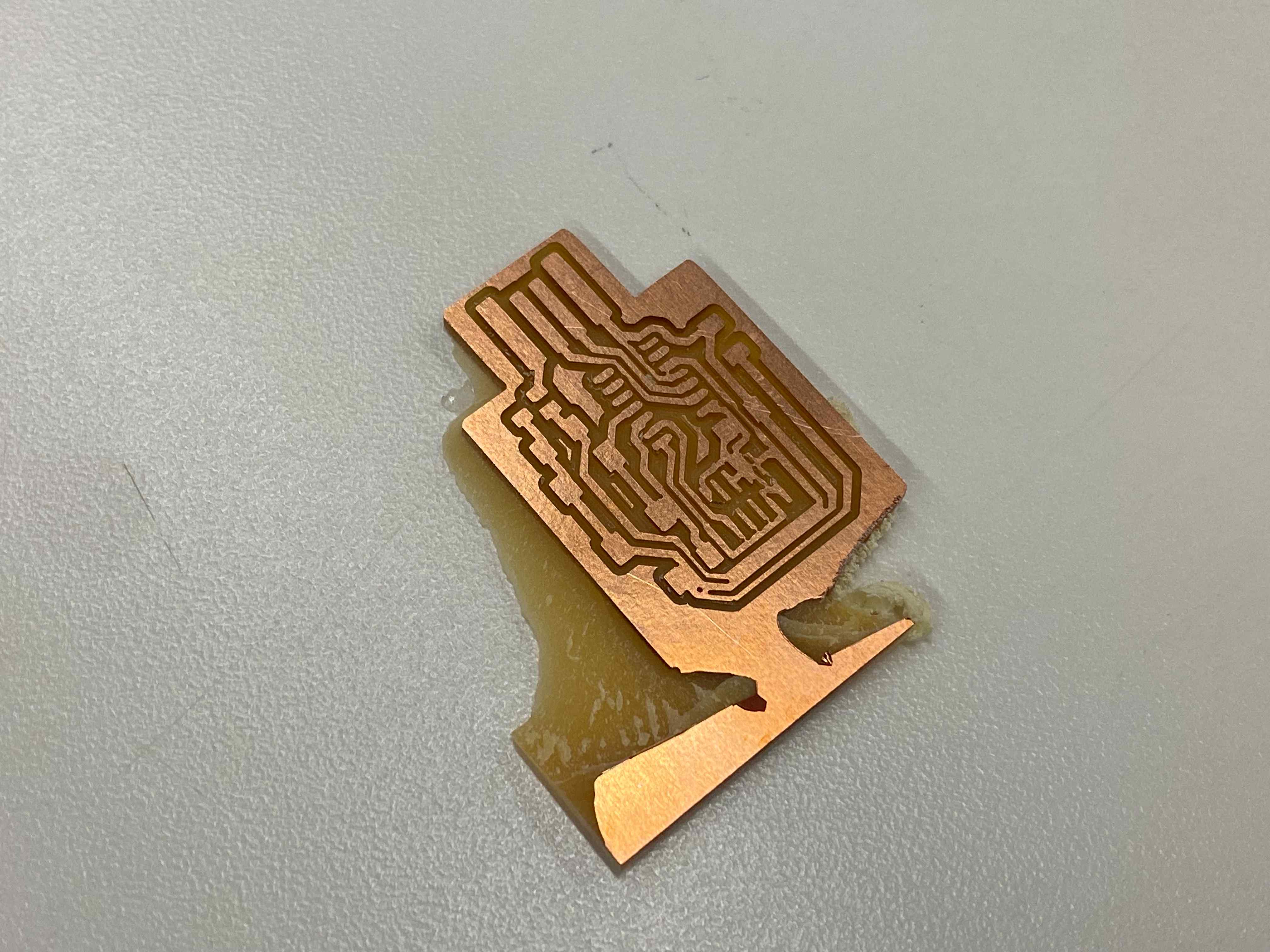
It turned out that my traces were very close together, so some routes were not able to be milled. I used an x-acto knife to hand-cut these routes. Eventually I was able to stuff the board successfully. Since the 5x2 header footprint was so thin, I tried using solder paste with a heat gun, and it worked like magic!
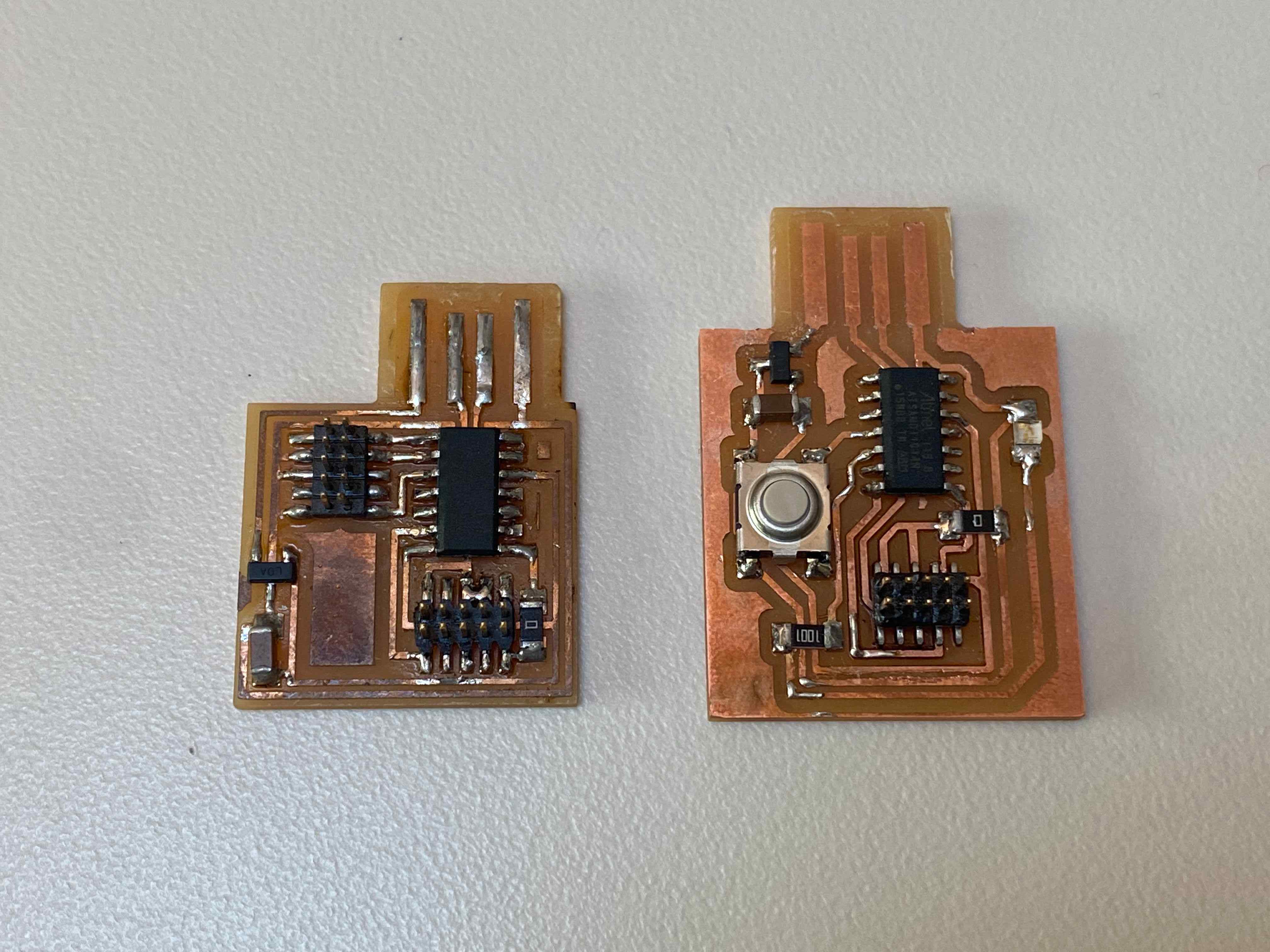
The new board (right) alongside the old board (left). I followed Leo's tutorial to use openocd to program my board. With my functioning programmer from Week 2, this was no problem.