Week 07 - Embedded Programming
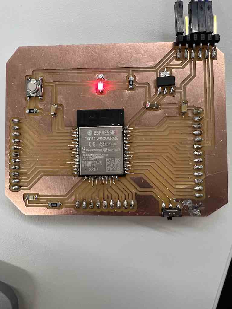
This week I decided to design a new board to be able to program more complex tasks with more connections and make it for my other assignments. So I decided to design a PCB using ESP32 prossesor
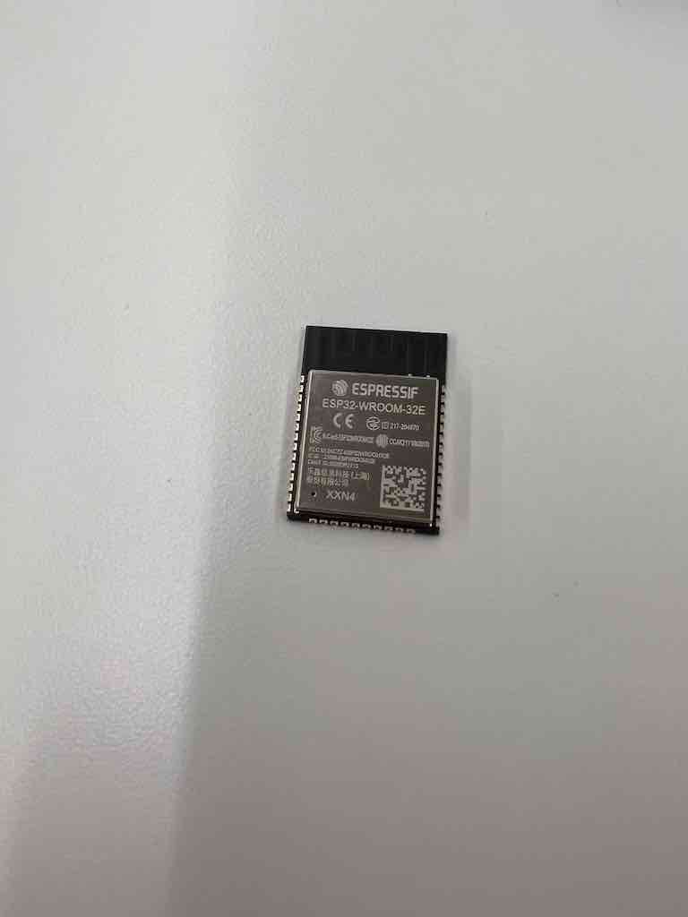
I used the help of a previous desgin to make my schematic and design my board for the ESP32.
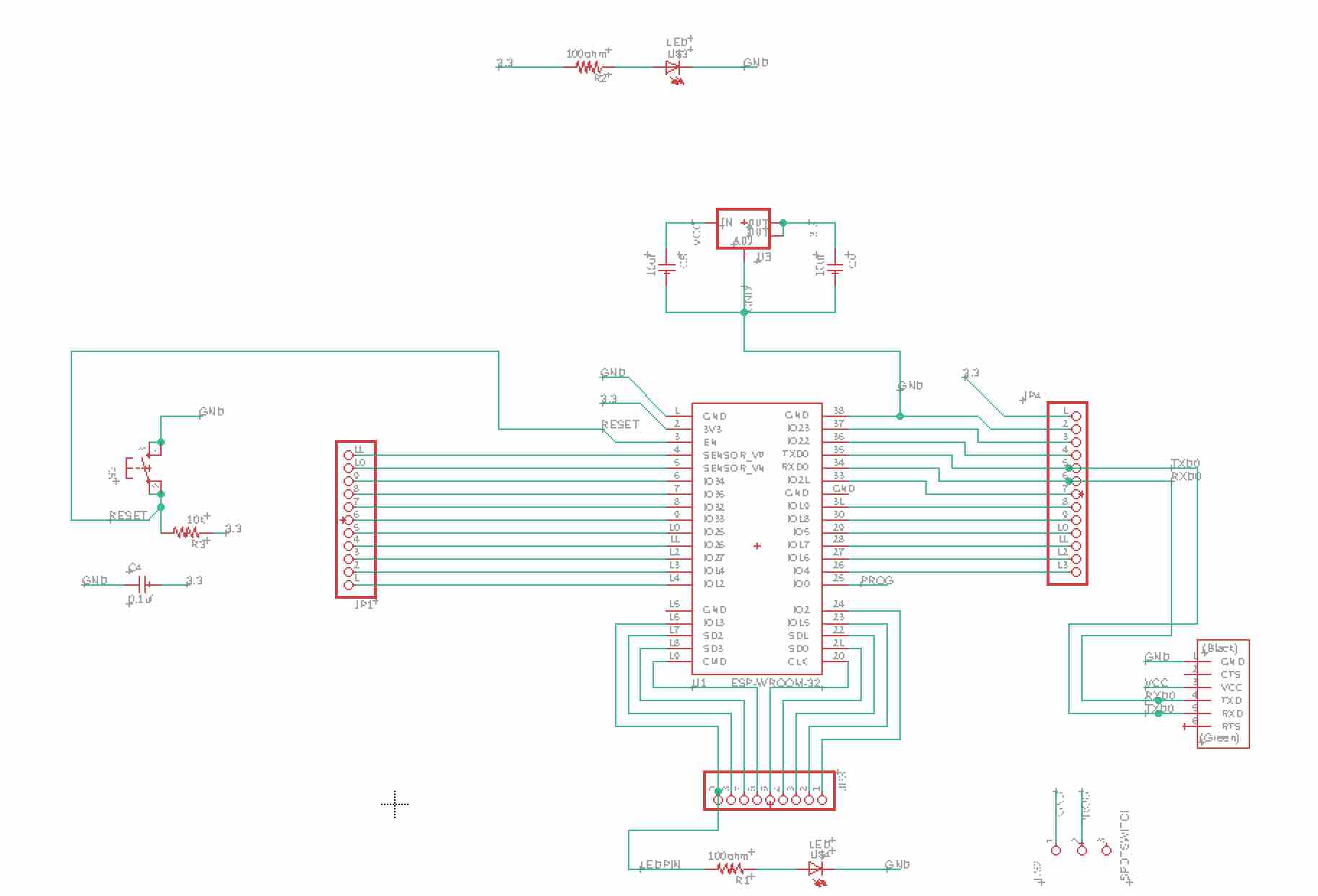
This is the schematic for my board using eagle in fusion 360.
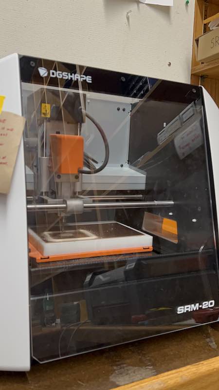
I milled the board.
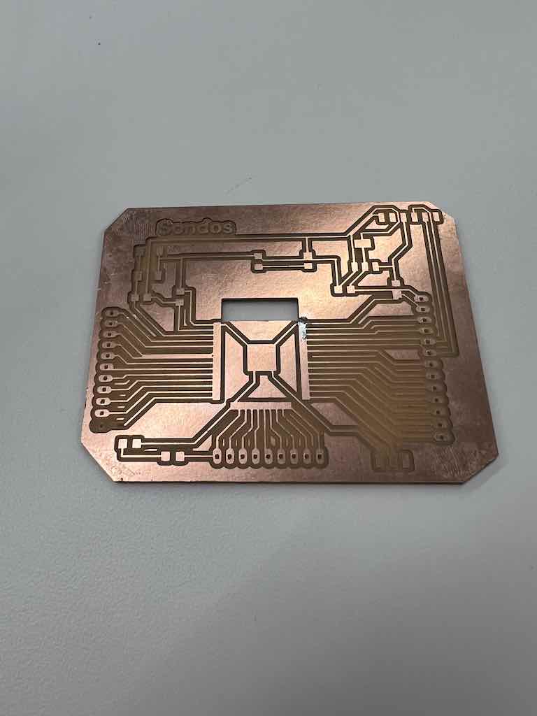
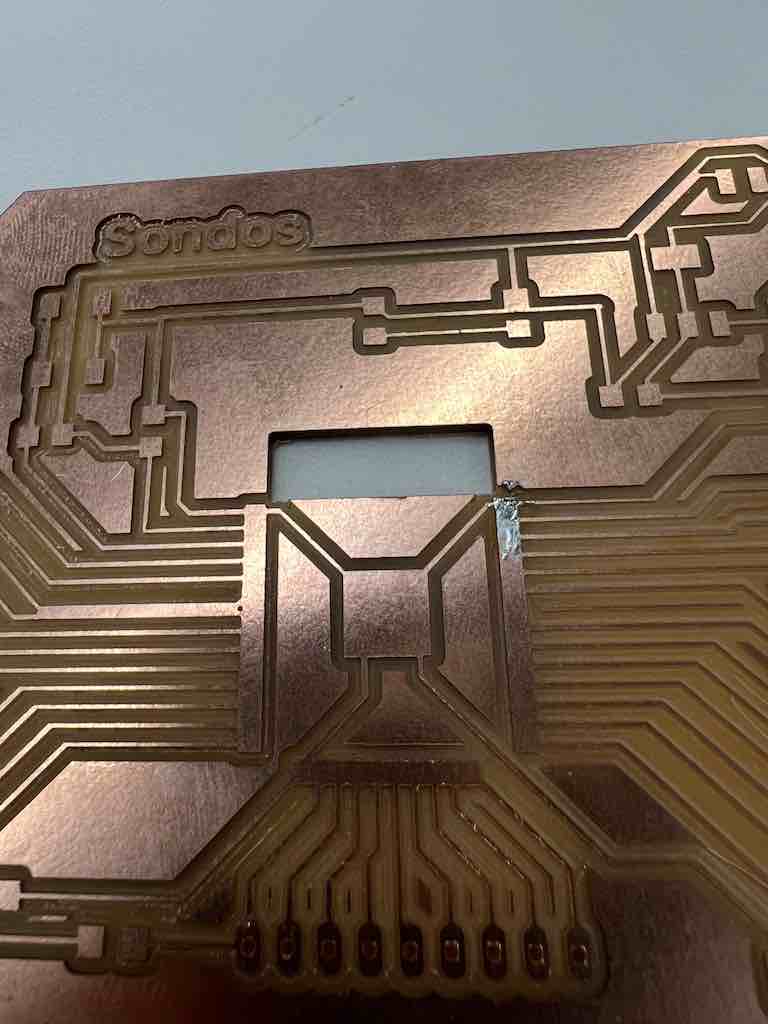
But the pads came connected because the clearance between them wasn't enough for the drill pit to clear and mill through.


So I had to adjust the footprint of the ESP32 that I used, to adjust the clearnace between the pads, you can see the differenc ei n the size between the first and the second pad
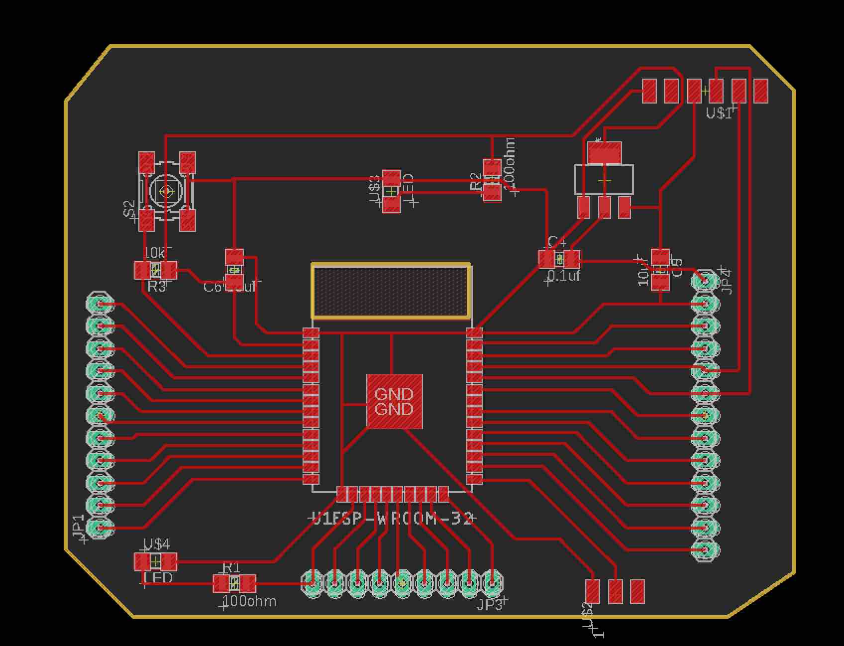
I made sure the clewrance was 17 mil and there was clearance between the pads, and made the tracings for my PCB.
Here is the final design of my PCB, ready to be milled. I milled the traces, then holes, then outline.
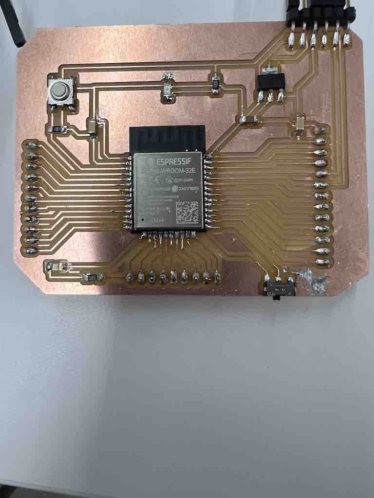
Then I milled the board again and it worked and I had clearance required for each pad to be seperate, and I was able to solder the parts.
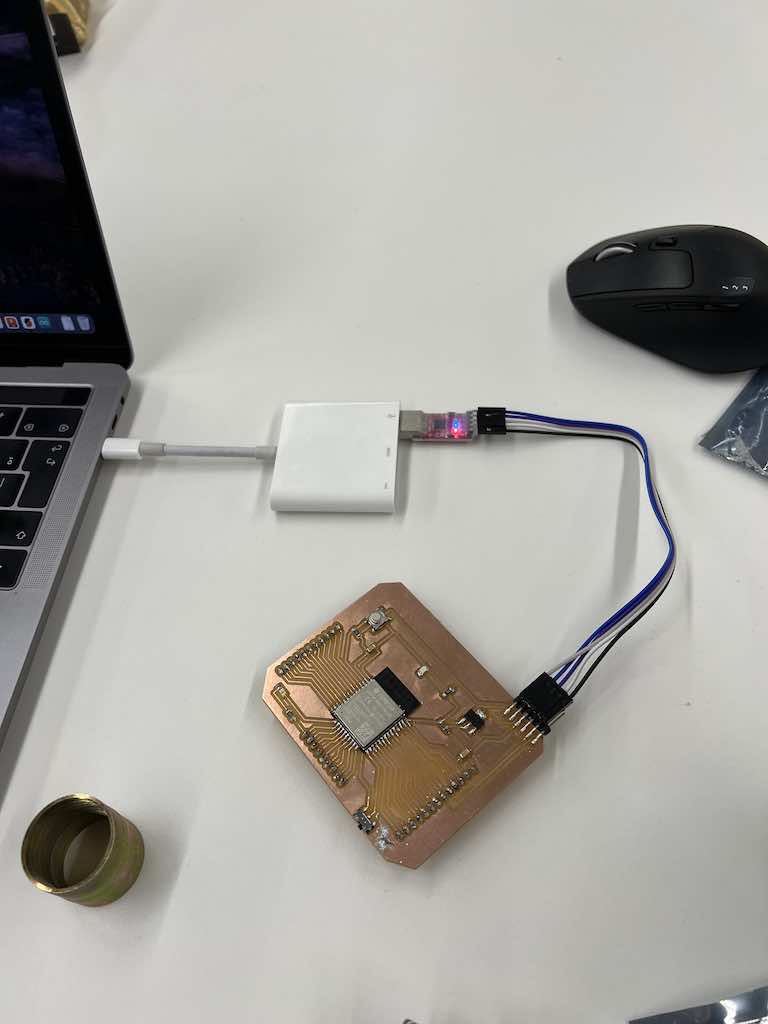
I used the connection to connect the board to my laptop and programmed it to light the LED.

And this is the final look of my board, with the LED on. And I will use it to program other sensors for my next projects