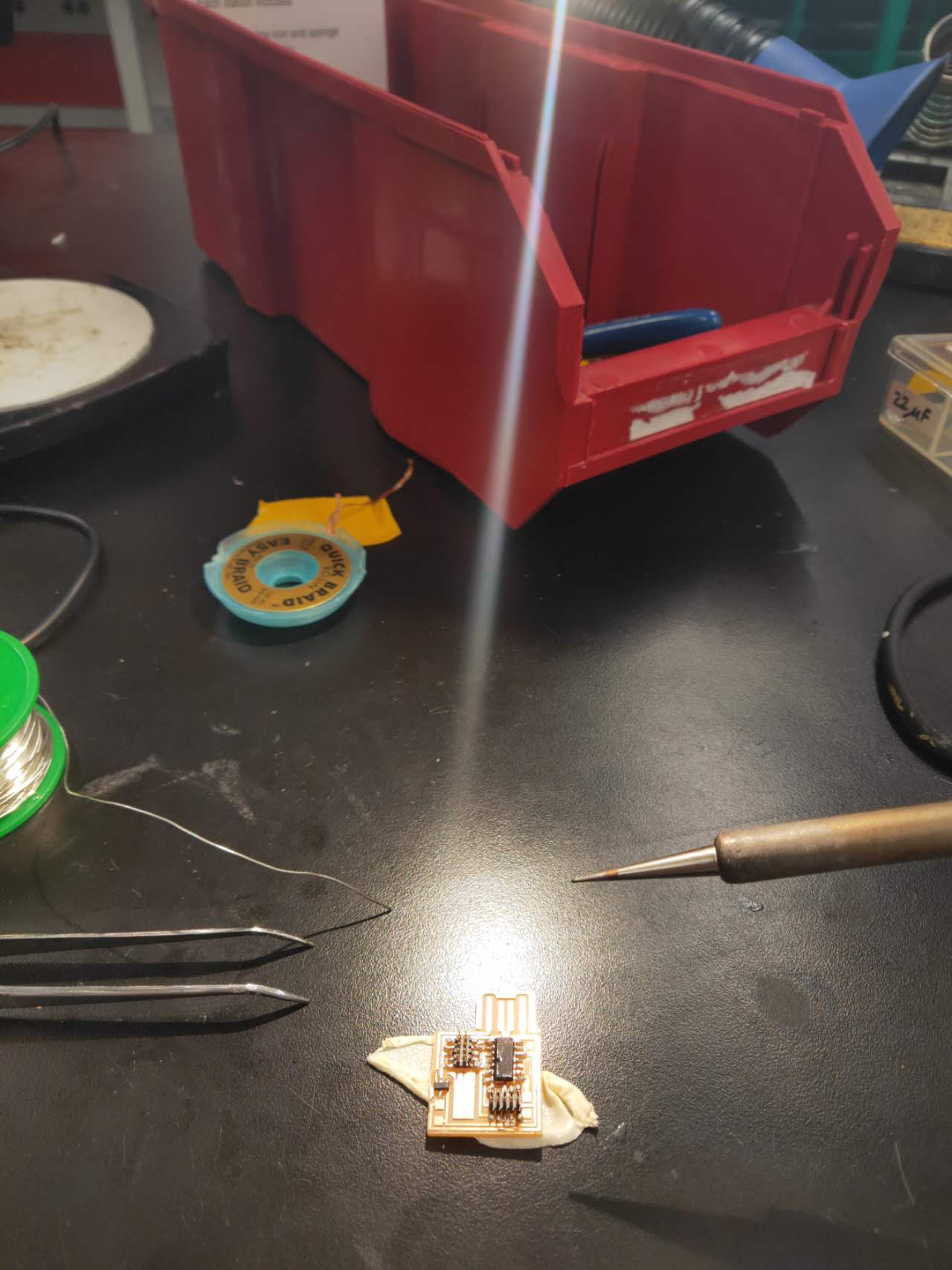
The third week we are tasked with making PCBs. For this week, we are not doing anything creative. We just have to make sure we have a "programer" which works, and everything should be following the template provided online. First we have to learn how to use the mini mail. It is a machine with an orange cover. We have to use two different drill bits of different sizes. The thinner drill bit is for engraving the circuits on the copper plate. The thicker drill bit is for cutting the circuit board's perimeter out. I had a lot of issue with the software because I keep triggering the machines failsafe. But eventually, I managed to cut out a identical board from the templates.
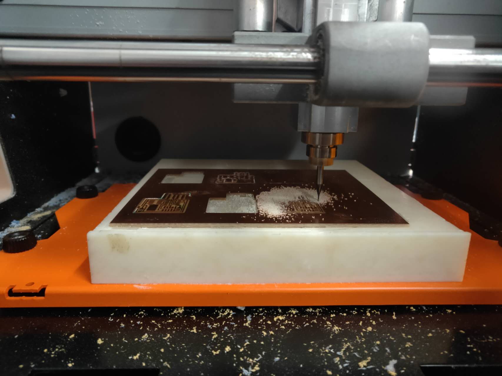
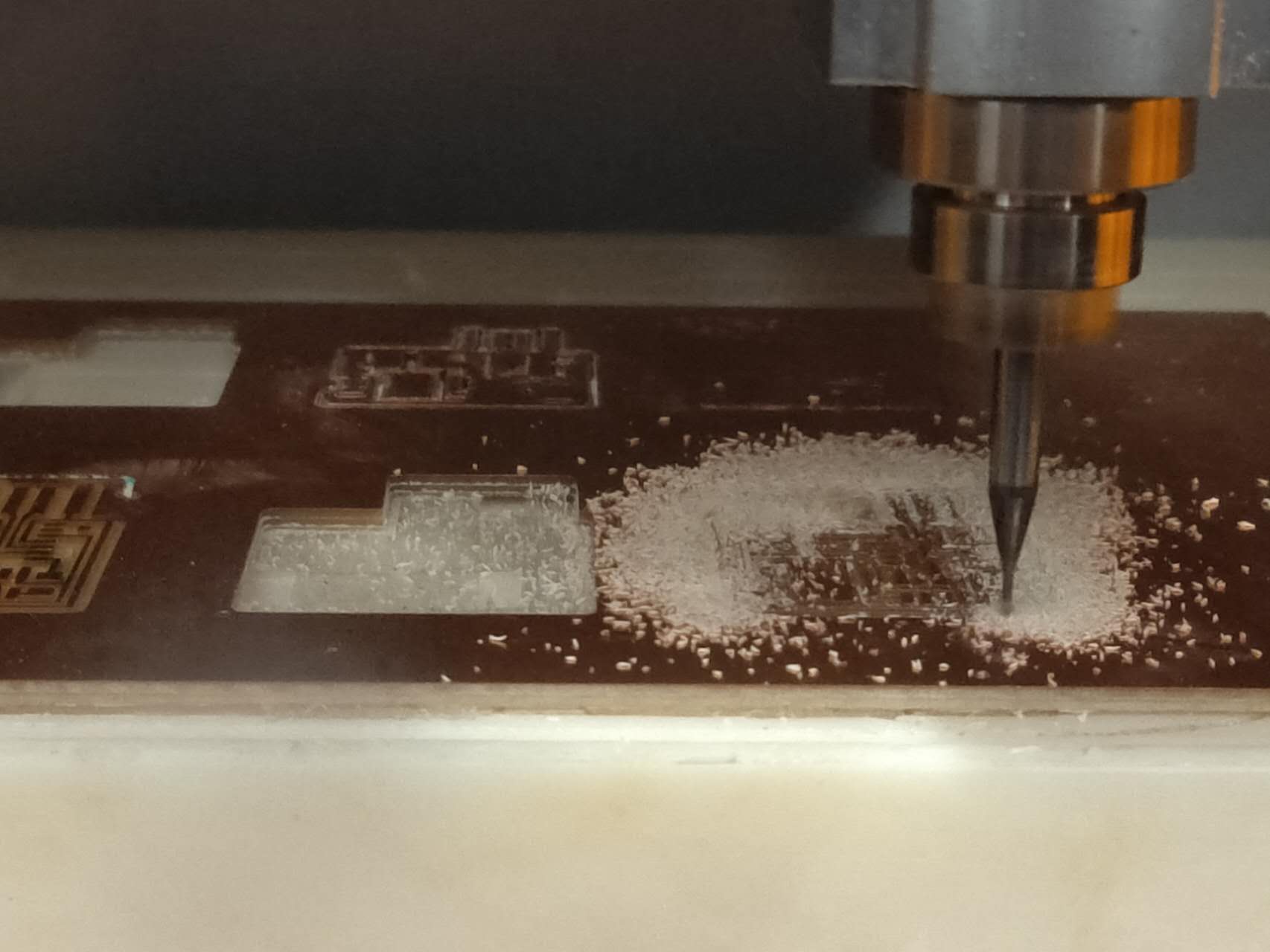
The third week we are tasked with making PCBs. For this week, we are not doing anything creative. We just have to make sure we have a "programer" which works, and everything should be following the template provided online. First we have to learn how to use the mini mail. It is a machine with an orange cover. We have to use two different drill bits of different sizes. The thinner drill bit is for engraving the circuits on the copper plate. The thicker drill bit is for cutting the circuit board's perimeter out. I had a lot of issue with the software because I keep triggering the machines failsafe. But eventually, I managed to cut out a identical board from the templates.
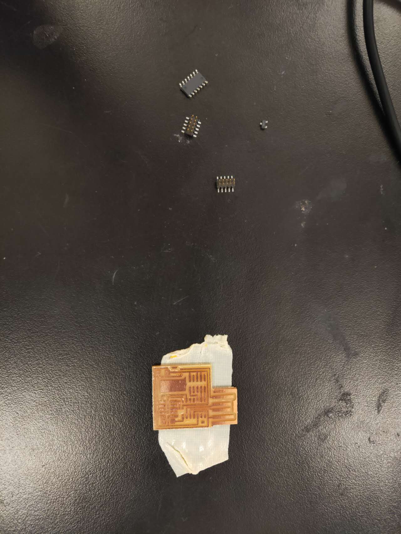
The board is ready for soldering. We need to solder on capacitators, resisitors, processors, and other things. To be honest, I have little clue of what I am doing. I learn to read some of the labels from the circuit diagram.
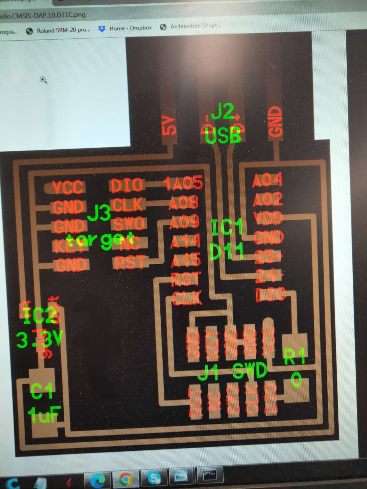
From the reference image, I understand that D11 is SAMD11 processor. C1 is capacitator. R1 is resistor. I have to ask my peers for other things which I can't identify. Also, it is quite important to get the SAMD11's orientation correct. From reading the manual, we can see there is a dot labeling it should be placed with the dot facing upper left. We can understand the orientation by locating 3 pins from the manual to the board diagram: the GND, RST, and VDD. I still need to learn more about the labels and components.
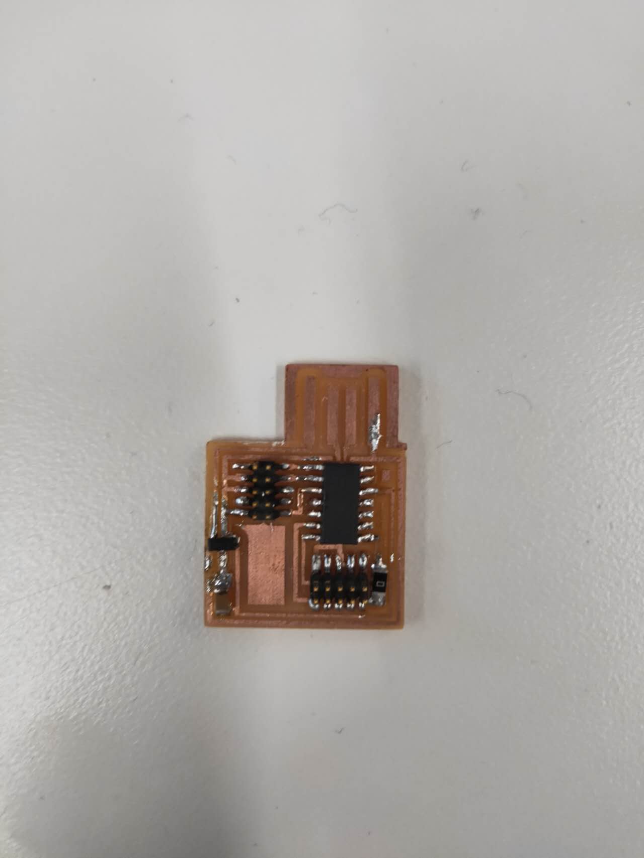
The soldering takes awhile to learn. I kept messing up because I put too much solder. Then I realize it is important to pre heat the "feet" and the plate. If the feet of the components are hot and the copper plate is hot, the lead wire just melt so nicely on to the joint and wraps around them. I have to use hot air gun to de-solder a component because initially I melted too much solder on to the connection and the solder runs underneath the component, which creates a short. I also used a copper mesh wire tool to desolder, but it has been super hard because it takes awhile to heat up the solder through the copper mesh. Lesson learned that it is always easier to solder then removing solder.
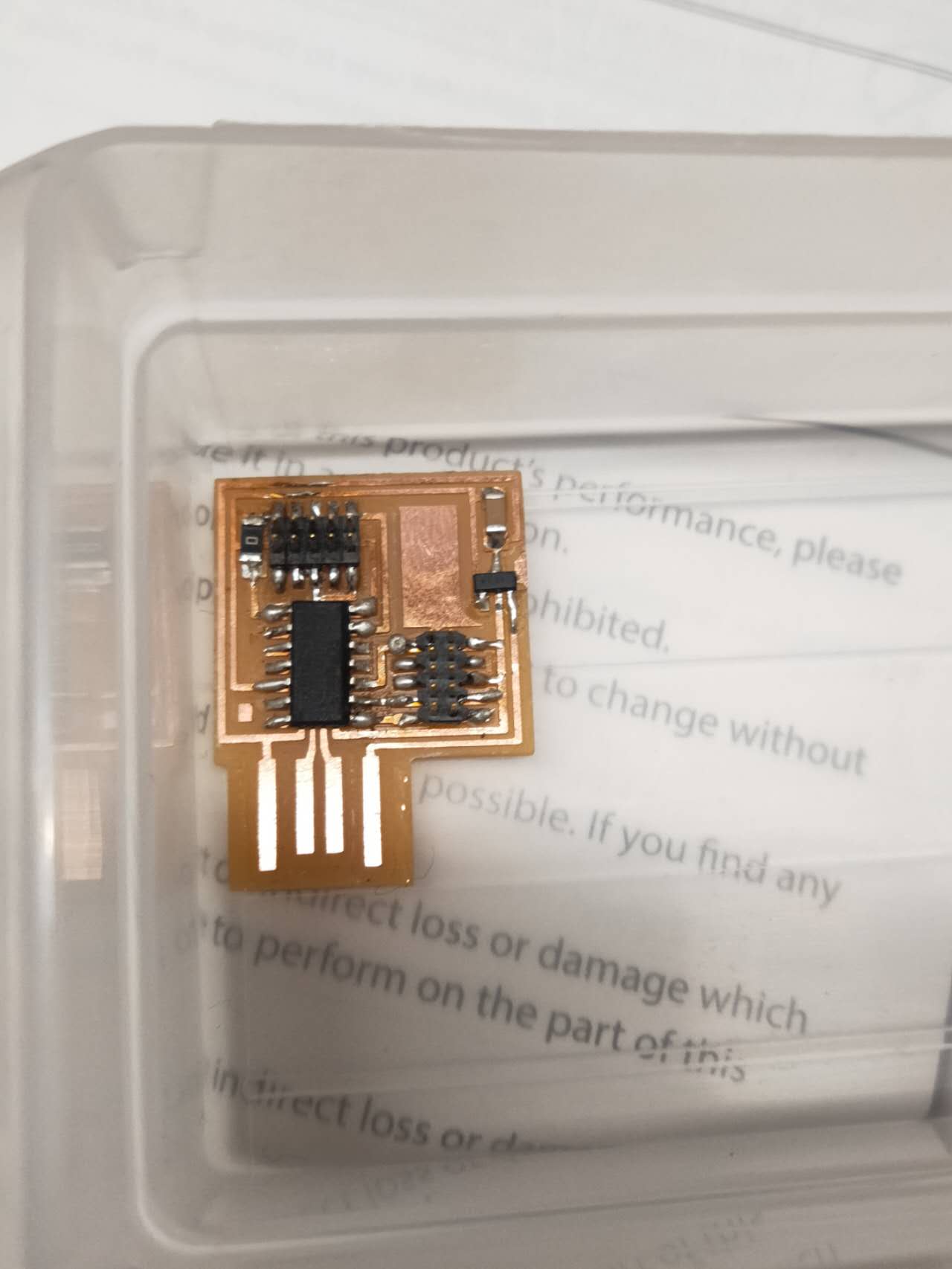
After checking all the connections with multimeter by following the board diagram, I made sure all the circuits are good with no shorts. Then, my peers and TA help me to program my board into a program. I have to add more solder on the usb connecter, but after that it doesn't seem to be too difficult. My pcb is finally programmed, and I will learn the fundamentals of command prompts in later weeks!
Here is the link to download the png pattern to cut your pcb!
Download Template 1 Download Template 2