
This week’s GROUP assignment was to characterize the design rules for in-house PCB board production. This was necessary to detemine the contraints for on how thin the traces that connect the components on our PCB board can be.
Working with the entire Harvard Section, we started by printing a comb with our CNC cutter, incrementing the width of the comb's teeth from 1 mil to 20 mils. Our goal was to determine our CNC machine’s smallest dimension for cutting a functional PCB. Through our different variations, we determined traces thinner than 8 mils had a high risk of breaking and therefore could not be trusted. Additionally, a gap of 16 mils was the minimum limit between traces.
We also tested the milling bit sizes and tried using a 1/32-in end mill instead of the suggested 1/64-in end mill for cutting traces. The larger bit cut unusable traces for all size increments with this test comb, so much so that we quit the job before it finished. To use this bit, traces would have to be much larger than ones created with the suggested 1/64-in end mill, which doesn’t make this design choice functional for most PCB applications.
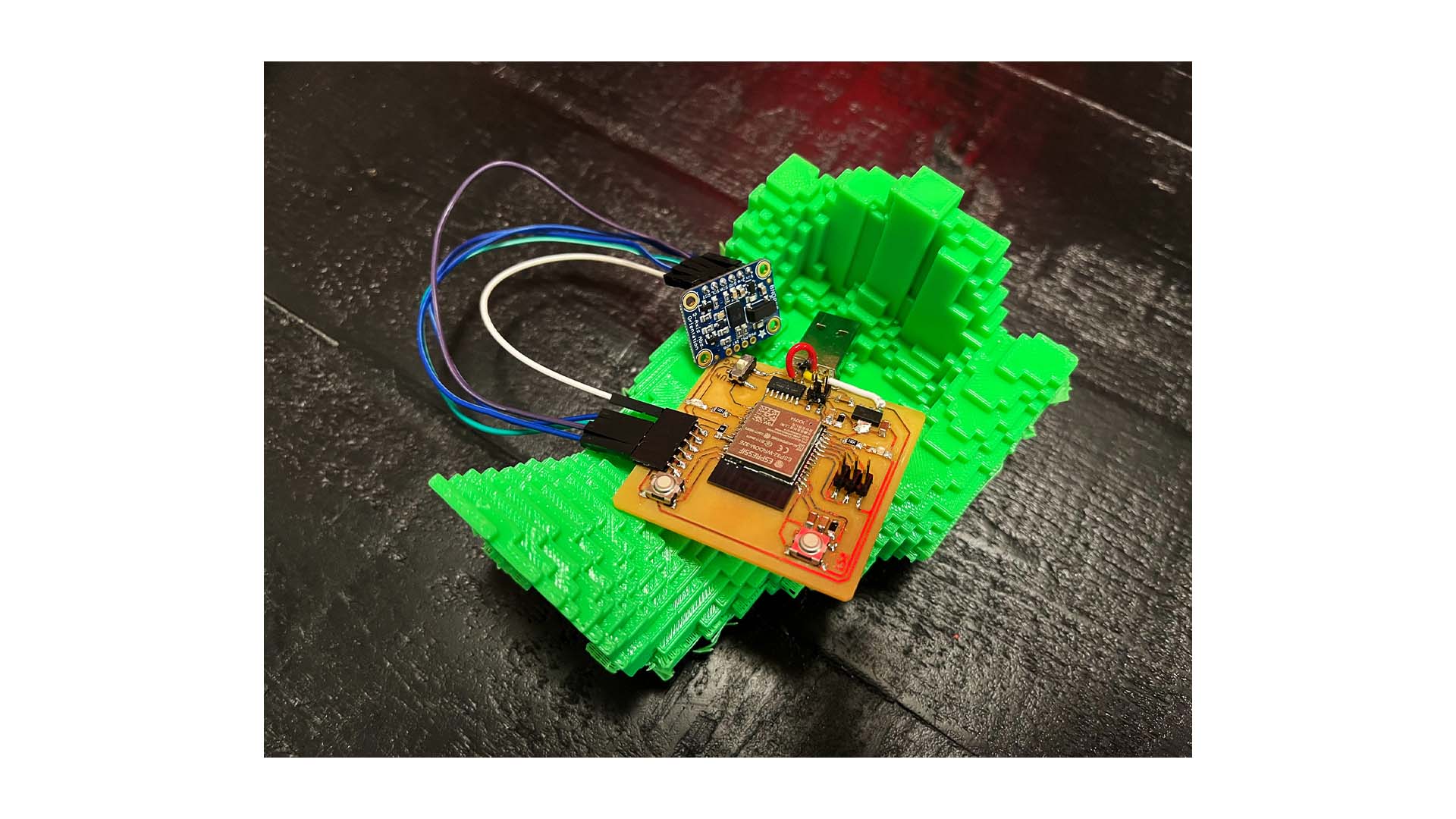
Individually, we were assigned to make an in-circuit programmer that includes a microcontroller
I started using MODs to vectorize my PCB design and printed out the board on the CNC machine. Initially, I was too sensitive with the end mill’s placement on the copper plate, so my first pass didn’t even cut into my material. Once I got a hang of installing the mill in the machine, it was smooth sailing for cutting the traces and the outline of the board. I decided to cut two boards in case I had an issue during my soldering process. Next, I had to remove the remaining copper around the tip of my USB connection which was not removed by the end mill. It would be ideal if this part of the process could be circumvented by altering the design of the vectorized CNC path.
I was concerned about the soldering process because friends of mine have complained about the tedious process. Despite my hesitation, I enjoyed learning by practicing on old and broken boards that I found around the shop. After I felt comfortable, I acquired the components needed to complete the board and began attaching them. At this point, it became a kind of iterative process as I misplaced a few items and had to remove them and rearrange the structure. The copper braid, used to remove solder, took some practice to use but came in handy for cleaning us my mistakes from beginning to end. After about 45 minutes of trial and error, both boards made it out alive!
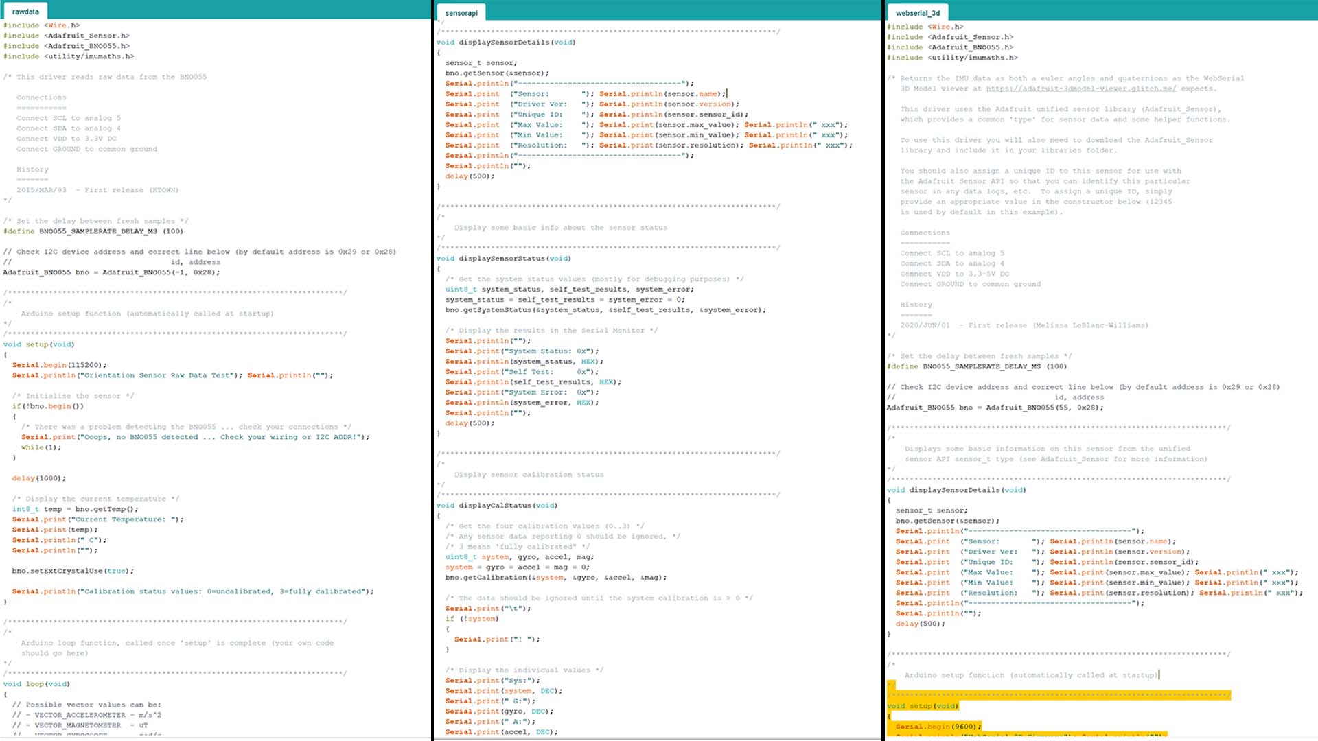
Lastly, I needed to install and burn Openocd onto my finished PCBs. This required a PCB already programmed with OCD, which I found in the lab. Next, I connected the two boards through the two 2x5 pin head connectors with a cord and attached them both to a power source (which was my computer). Once attached, I ran Openocd on my computer, and possibly out of pure luck, they both worked! I ran the Arduino bootloader to program them, then Free-dap to burn that program onto the boards. Since I use a PC and assisted others with Macbooks, I learned how to execute the process on both OS (Macs need Homebrew). But luckily, this was the only challenge I encountered in the programming process of the electronics production section.
This was a fun way to jump into circuit boards and CNC milling. I am looking forward to being able to design my board and learn more about the details of determining the architecture for the PCB I need for my final project.
Ideally, I will feel comfortable not only building the boards but understand the placement and detials of the components