I have some experience with electronics kits and soldering, but I have never made my own pcbs or had to determine how electronics should fit together. This proved to be the most difficult thing for me to complete, as I really struggle with working while being unsure. All the experience I've had with rapid prototyping has worked with me having at least a vague idea and/or understanding of what I am trying to achieve and how it would work. I have completely no idea how or why things work with electronics, and this lack of intuition makes it really hard for me to progress.
Working with Eagle
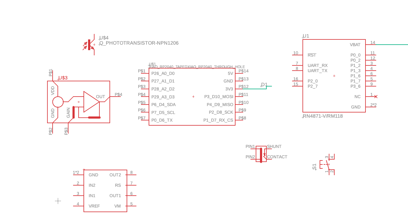
First, I began by downloading the Eagle library and trying to work within Fusion. I already do a bunch of CAD-ing in Fusion360, and I am rapidly running out of space on my computer, so I felt that working in Fusion would make the most sense. I really want to start working on and considering what will be needed for my PCB for my final project, because other than that I have no ideas for reasonably difficult projects that utilize PCBs. I then made a list of components/capabilities that I wanted my PCB to have.I also spent some time looking through the library to take note of what kinds of components would be available, what they do, and how they could be useful. After selecting the components I wanted to focus on, I tried to look up the part numbers so that I could find a datasheet with sample circuits. Now this is where things started to get stressful. I wanted my final project to have bluetooth capability so that it could have a remote that I could move around my room as I pleased. However, I could not entirely make sense of the datasheet, and I just generally felt unsure that what I was designing was going to work. This really crippled my confidence because I just always felt that I was wasting time. After a couple days of dreading working on the PCB, I spoke to one of the TAs, who helped me simplify, and also explained that there were some things that were not available in Fusion, but were rather available in KiCad. So, with that, I moved into KiCad. I will note that in hindsight, I did make some progress in Fusion, as shown below.
Parts in the schematic that I wrote out in Fusion360
Moving into KiCad
Speaking with Niklas Hagenann and classmate Simon Lesina Debiasi really helped me develop a better understanding of how I should go about this week, especially with my lack of experience. As I was designing, I was super hesistant because I was nervous that if I included the wrong resistors, forgot to include capacitors, etc that I would fry the microcontroller or worse still, fry my computer. (I imagine an experienced electronics person would say that I wouldn't possibly be able to accomplish that, but hey, better safe than sorry). I was also nervous about the finality of making a PCB - if I forgot a component, it wouldn't be as easy as just adding it on the breadboard, I would have to make a whole other PCB. So when they gave me the advice to start by making a little breakout board for my microcontroller, it made a lot of sense to me.
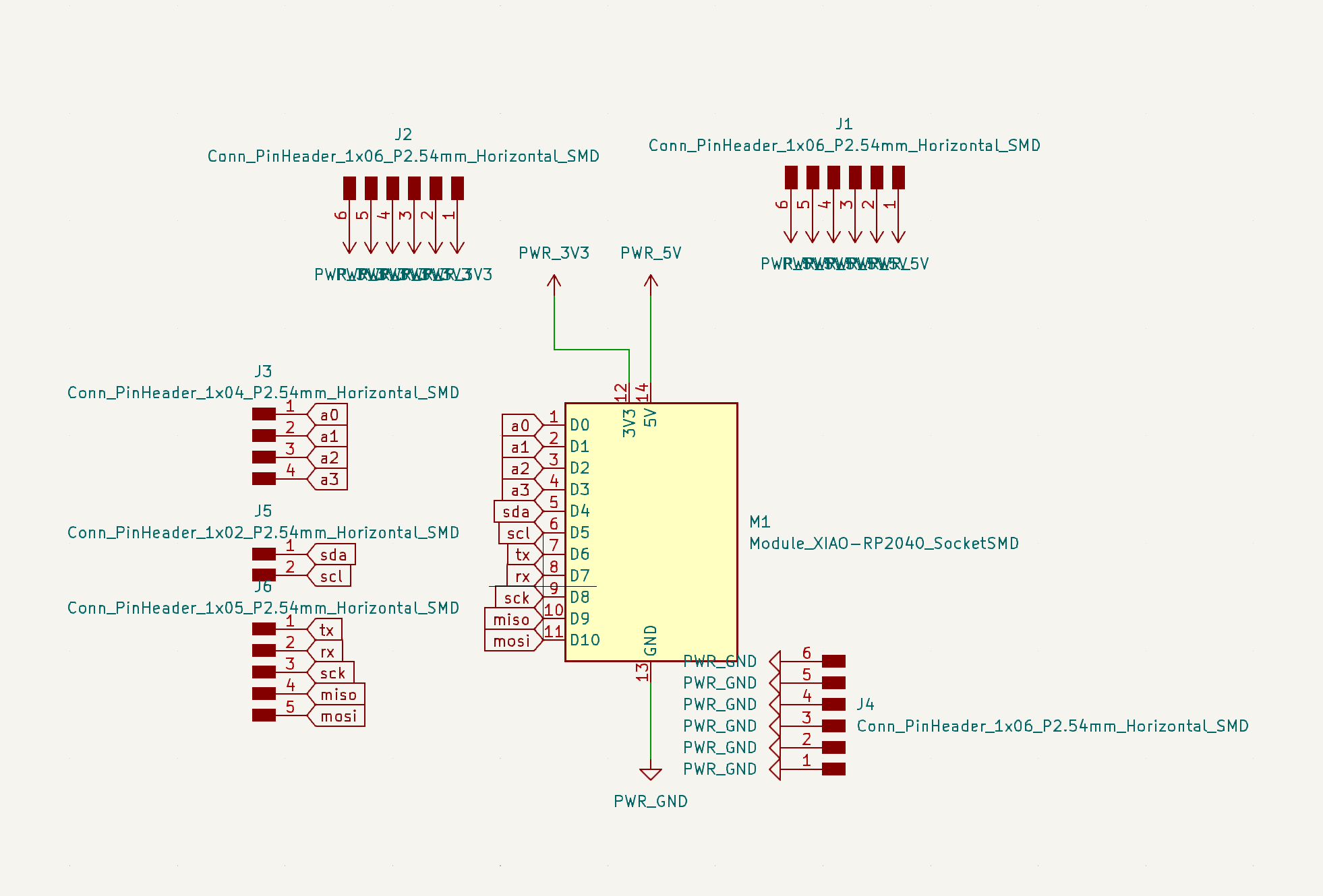
Moving into KiCad, I had access to a bunch of horizontal male connectors that I could plug jumper wires into. Looking back at the pinout sheet for the XIAO RP2040, I decided to try and group the pins that I wanted to be next to each other. It came together pretty easily - I put all the analog pins together, the I2C pins and then grouped the remaining pins that seem important for some kind of communication (although to be completely honest I have no clue what they do). Then, I figured I should have multiple connectors to ground because almost any component I would add to it would need to connect to ground. Then I used little connectors that could be attached to my XIAO RP2040, so that I would not have to permanently solder it into the board. After putting all of this together into a schematic, it looked like this!
Board Schematic as designed in KiCAD
Routing the board
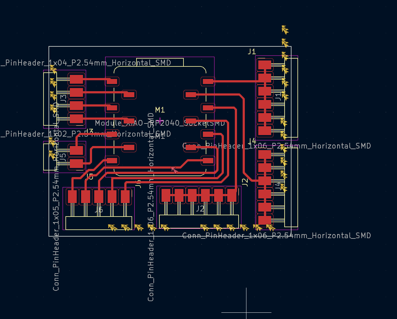
From there I moved into the PCB editor. Upon Niklas's advice, I set the width of my traces to 0.4 mm and the minimum spacing to 0.5 mm. Working with connectors instead of rigid connections meant that for the most part, any problem with the routing could be fixed by simply switching which connector pad was connected to which end. This showed me that it was incredibly helpful to use labels instead of nets in the schematic (a helpful tip from Simon), as it was super easy to switch the position of the labels instead of having to redraw the nets. I also realized looking at the PCB that I oriented the horizontal connectors backwards in the schematic, so while the order in which I had assigned things made sense in the schematic, when I put it in the PCB editor, it was impossible to route. Once I had arranged things in a way that I could see mentally solve the way that I wanted to route, I began doing the routing! After that I had my finished PCB design!