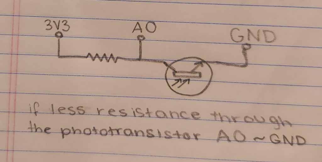
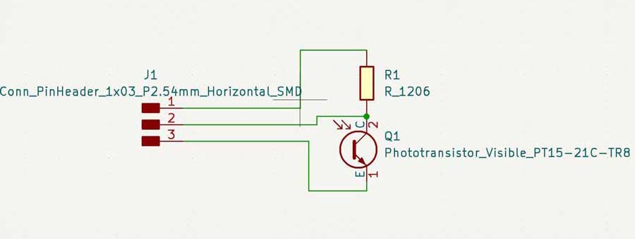
Going back to what things I would need to utilize to complete my final project, I wanted to learn how to use a phototransistor. I quickly drew up a little schematic based on what the phototransistor does (increase the resistance depending on the amount of light). I figured that the voltage drop across a resistor in series would change according to the resistivity of the phototransistor, which would give a way to determine whether the lights were on or off. It was pretty seamless to transition these ideas into KiCAD, and I just connected the points to 3 pin connectors so that I could use jumper cables to connect it to my previous breakout board for the XIAO RP2040.
Sketch of the Phototransistor
Phototransistor Schematic
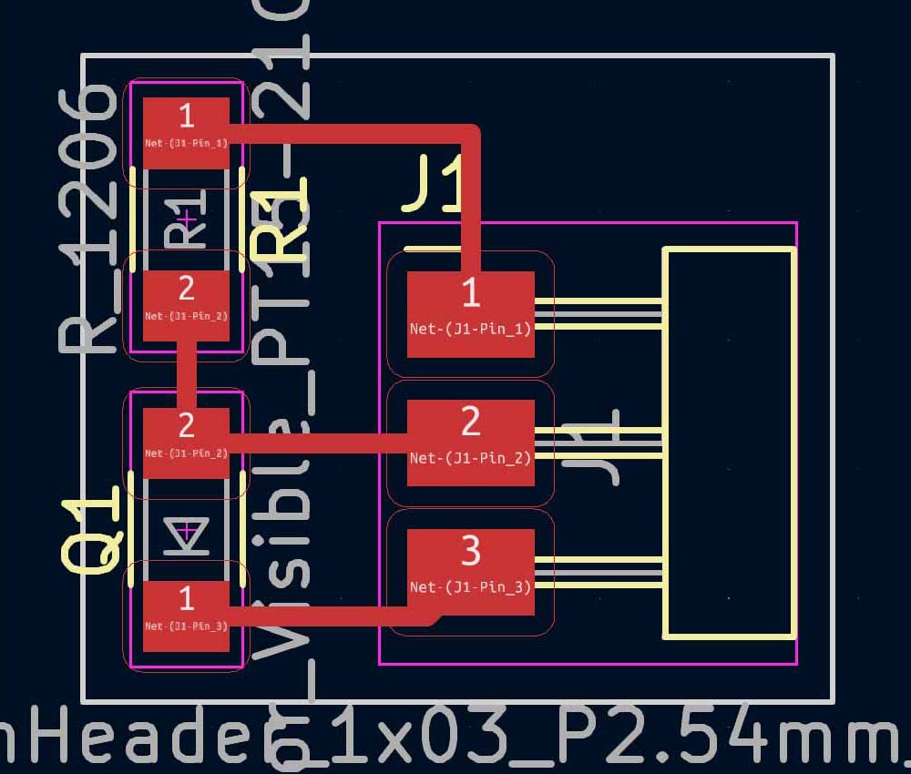
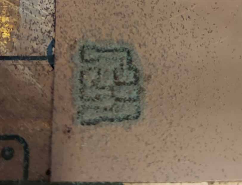
Phototransistor PCB
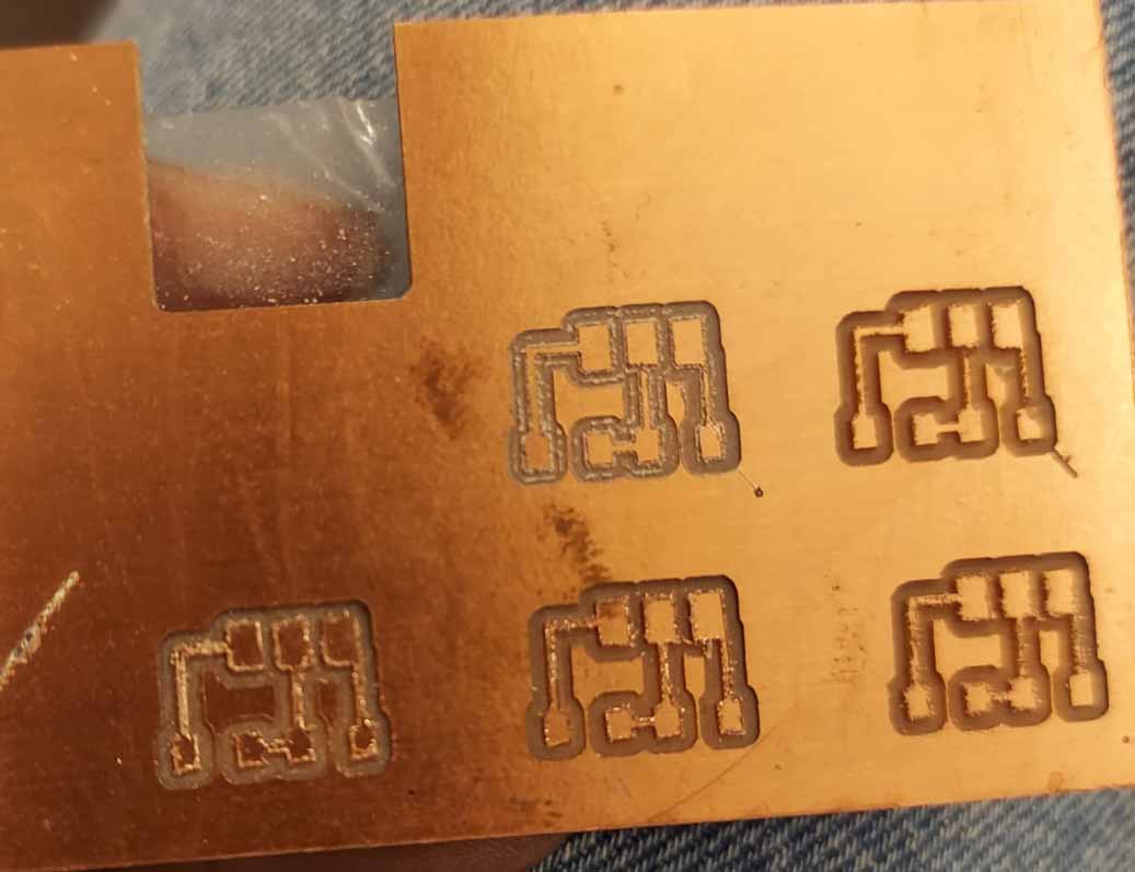
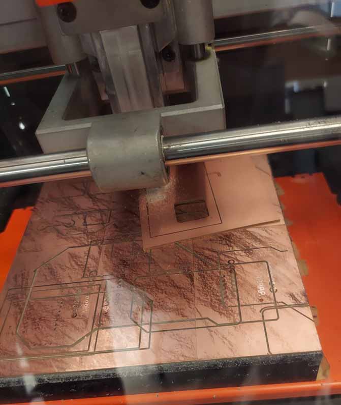
Milling the Module
As I was milling, I ran into a lot of issues. This was the first time I was running the machine entirely by myself, so naturally there were growing pains. As I loaded up the first job, I noticed that the endmill kept dragging against the copper. It broke the endmill, and it took me a while to determine what was wrong; it was set to jog at z=0. Honestly, it was pretty instructive to see what a broken endmill looks like. I then used 2 different endmills, but then the traces continued to come out super scraggly and unreliable-looking. Based on Jenn's advice it just seemed like the other endmills were a bit damaged (although the damage was not visible).
Despite trying with different endmills, the traces kept coming out poorly.
I was super frustrated, so I came back another day and used another endmill and it worked! I did have a small issue with a board not sticking down properly, but once I did a better job of using the double sided tape, it did not happen again. This second picture shows the traces before I vacuumed but they turned out much better.
The board moved while I was milling - a reminder to stick the board down as best as you can and with the tape as flat as possible
These traces came out much better!
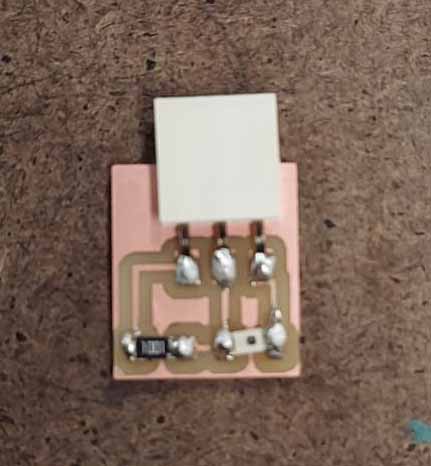
Soldering the Module
I looked at the PCB design a lot as I was soldering in the components. It was pretty straightforward, except for putting in the phototransistor. Based on the work I did making the LED/button module, I figured the polarity of the phototransistor would be marked similarly. After trying and failing to find the exact phototransistor data sheet, I thought the green spots pointed in the direction of electron flow, similar to the LED, and soldered accordingly.
Phototransistor Module
Testing the Input Source
After all of the milling, I tested the phototransistor module, and was disappointed to find that it did not seem to react at all to changes in light. Upon flipping the ground and voltage source, I found that the voltage that was recorded actually did change based on the light - which told me I had actually put the phototransistor in the opposite direction. However I did find that it was not very sensitive to light, so I wanted to also try increasing the resistance of the resistor. I then returned to the archshop, and granted that the PCBs were pretty small and quick to solder, I decided to make two of them so that I could make one with a 1kOhm resistor and one with a 10 kOhm resistor. This went a lot more smoothly than it did before as I'd had more practice with soldering the components, and I made sure the direction of the phototransistor was right before I soldered. I then decided tried to measure and it worked. Again, even using the largest resistor, it was a little less sensitive than I would have wanted, but I was able to read A1 and find that the reading changed a good amount as I changed the amount of light, as seen below.
Demonstration of the phototransistor module - the number goes up whenever I covered the module with my finger.