How to Make (almost) Anything 2023 | Week 5.1: Electronics Design
Home
Assignment: Group Project -- Use the test equipment in your lab to observe the operation of a microcontroller circuit board; Individual Project -- Use an EDA tool to design a development board to interact and communicate with an embedded microcontroller.
Individual assignment: Use an EDA tool to design a development board to interact and communicate with an embedded microcontroller
Description: After exploration of several EDA tools (KiCad, Eagle, Virtual Breadboard, Tinkercad), KiCad was used to design a simple development board with the goal of familiarizing myself with the layout and tools available for future designs.
Primary files:
- Electronics Design PCB schematic and design (KiCad)
Procedure:
- Explore various EDA tools (KiCad, Eagle, Virtual Breadboard, Tinkercad, etc.) and select EDA tool based on personal preference (I used KiCad)
- Import the fab academy library package for the associated EDA tool
- Create a 'New Project' within KiCad and select 'Schematic Editor' (note the schematic should focus on readability as the component layout can be altered at a later stage)
- Use the third button on right hand side to add a Xiao board to the schematic ("Module_XIAO-RP2040" was used)
- Search and add a connector to the schematic ("Conn_PinHeader_2x03_P2.54mm_Vertical_SMD" was used)
- Use the fifth button on right hand side to beging adding wires to connect the Xiao board with the connector (1->2, 2->4, 3->6)
- Search and add an LED and resistor to the schematic and connect the LED to the resistor, and connect the open end of the resistor to Xiao board pin 10 ("LED_1206" and "RP_1206" set to 100 Ohm value were used)
- Search and add a switch to the schematic and then use a wire to join the switch to the existing resistor, and connect the open end of the resistor to Xiao board pin 11 ("Switch_Tactile_Omron" was used)
- Search and add a ground component to the schematic and connect it the open end of the switch ("PWR_GND" was used)
- Search and add another ground component to the schematic and connect it to the Xiao board pin 13 ("PWR_GND" was used)
- Select 'PCB Editor' within KiCad once schematic is complete
- Slect 'Update PCB' on top ribbon to import schematic
- Set grid to 0.1in and move components to desired location (flipping components when needed to prevent wire crossing)
- Route the board using the 'Wire' botton on right hand side and tracing desired connection path between components
- Select 'Edge.Cuts' layer from right hand side and trace desired outline for development board
- When complete, export design as an SVG file, or Gerber for industry standard for manufacturing
Key learnings:
- There are many EDA tools available, which can be conveneint and overwhelming -- I spent majority of the week sorting through the different EDA tools trying to familiarize myself with the different nomenclature and which would be most intuitive for me to use; It is great that there are so many free EDA tools available, but I realized ultimately it is helpful to select one to get familiar with based on personal preference.
- Routing is an important consideration when designing your board -- When designing a board, it is important to consider the functional component of where the different connection points would need to cross and ensure they are routed in an effective path to reduce areas of crossed connections.
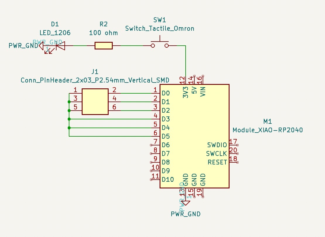
KiCad development board design - Schematic
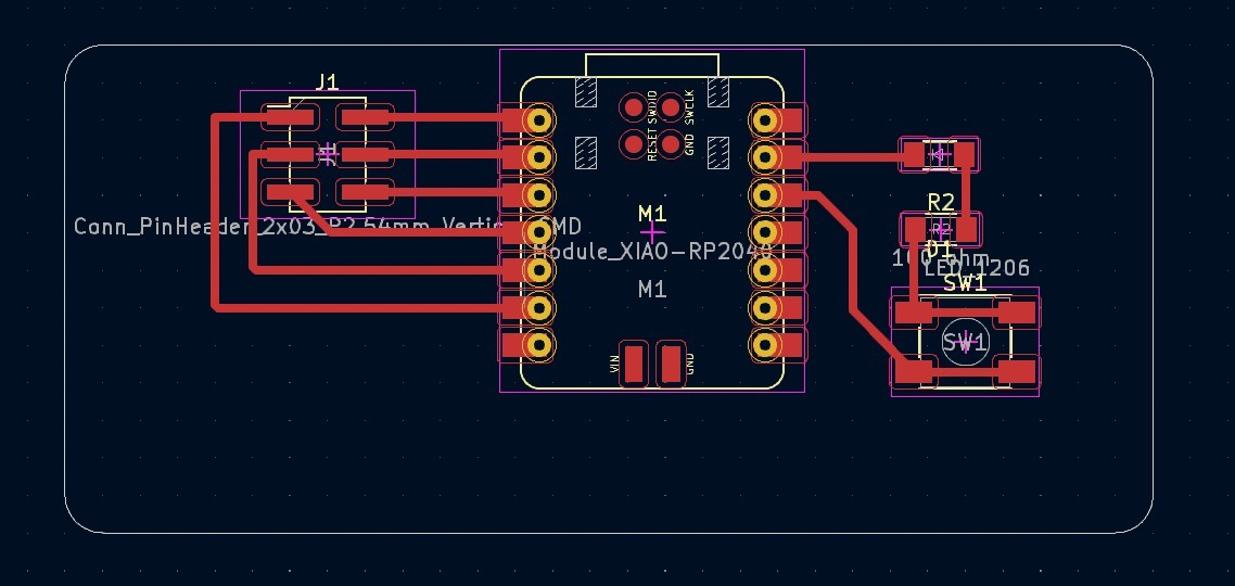
KiCad development board design - PCB editor