Inputs & Outputs
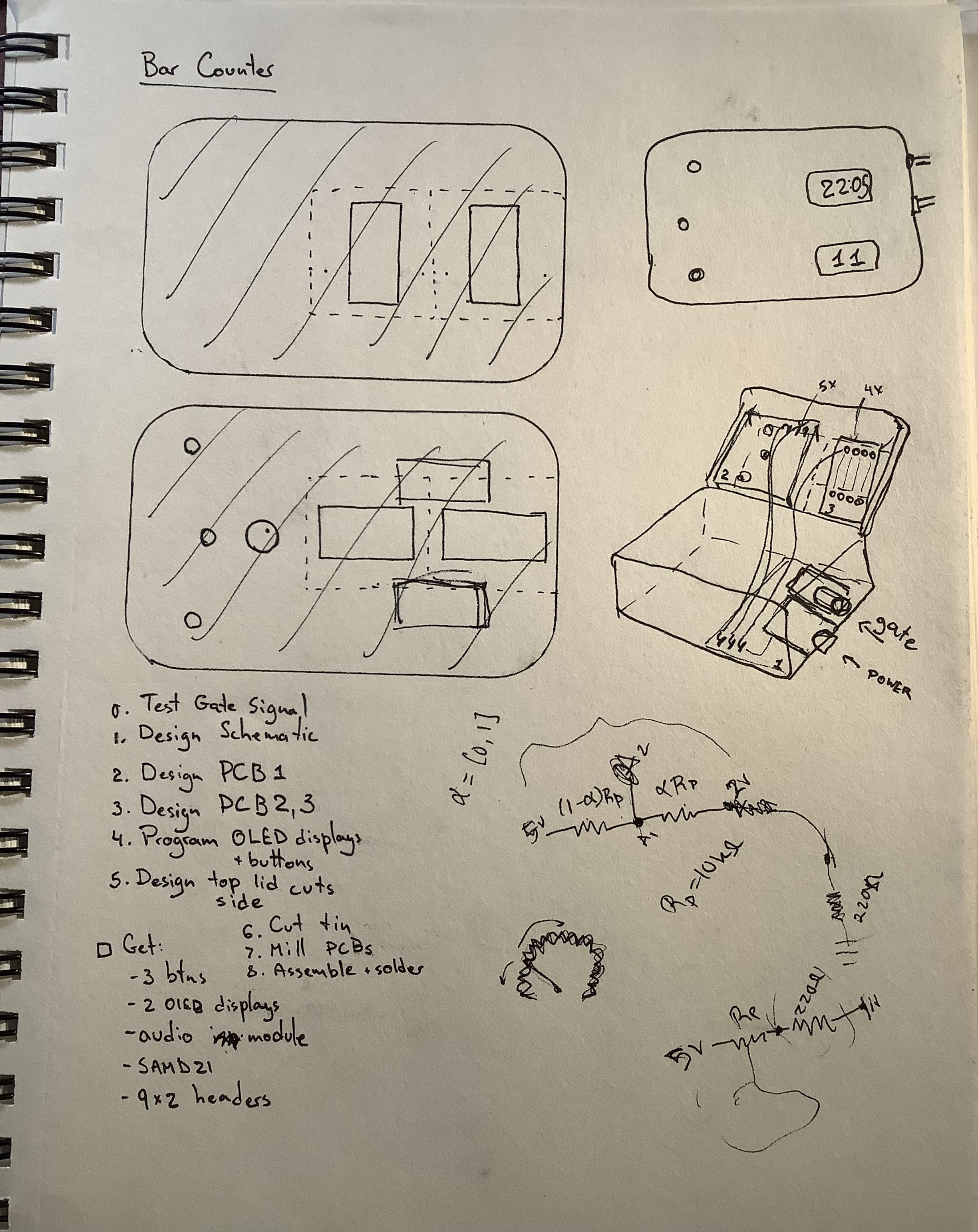
Making through holes:
Exporting:
Fabrication Outputs > Gerbers > Select F.cu (for copper) and Edge Cuts (for outline) > Plot
Also Generate Drill Files (for holes) with standard settings
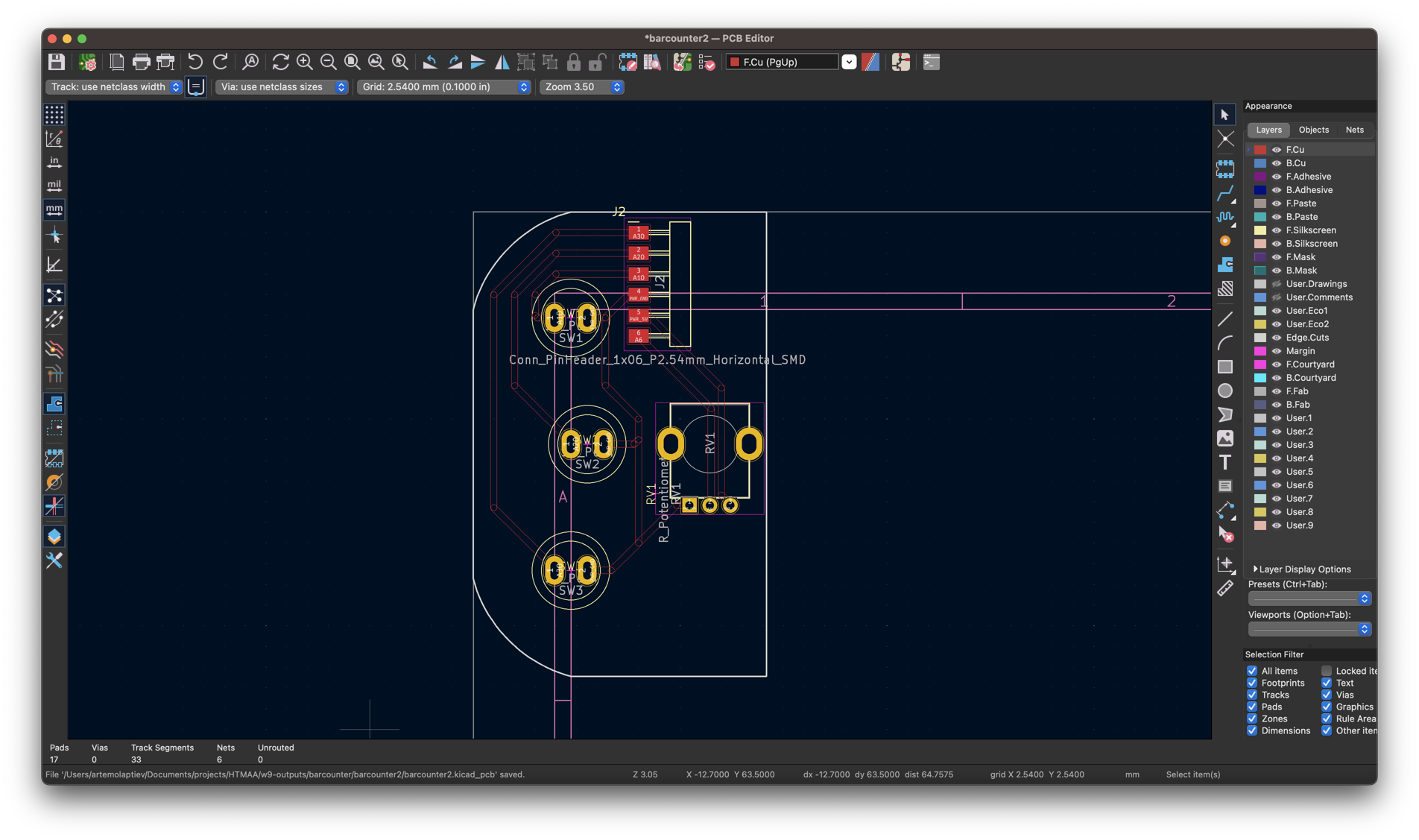
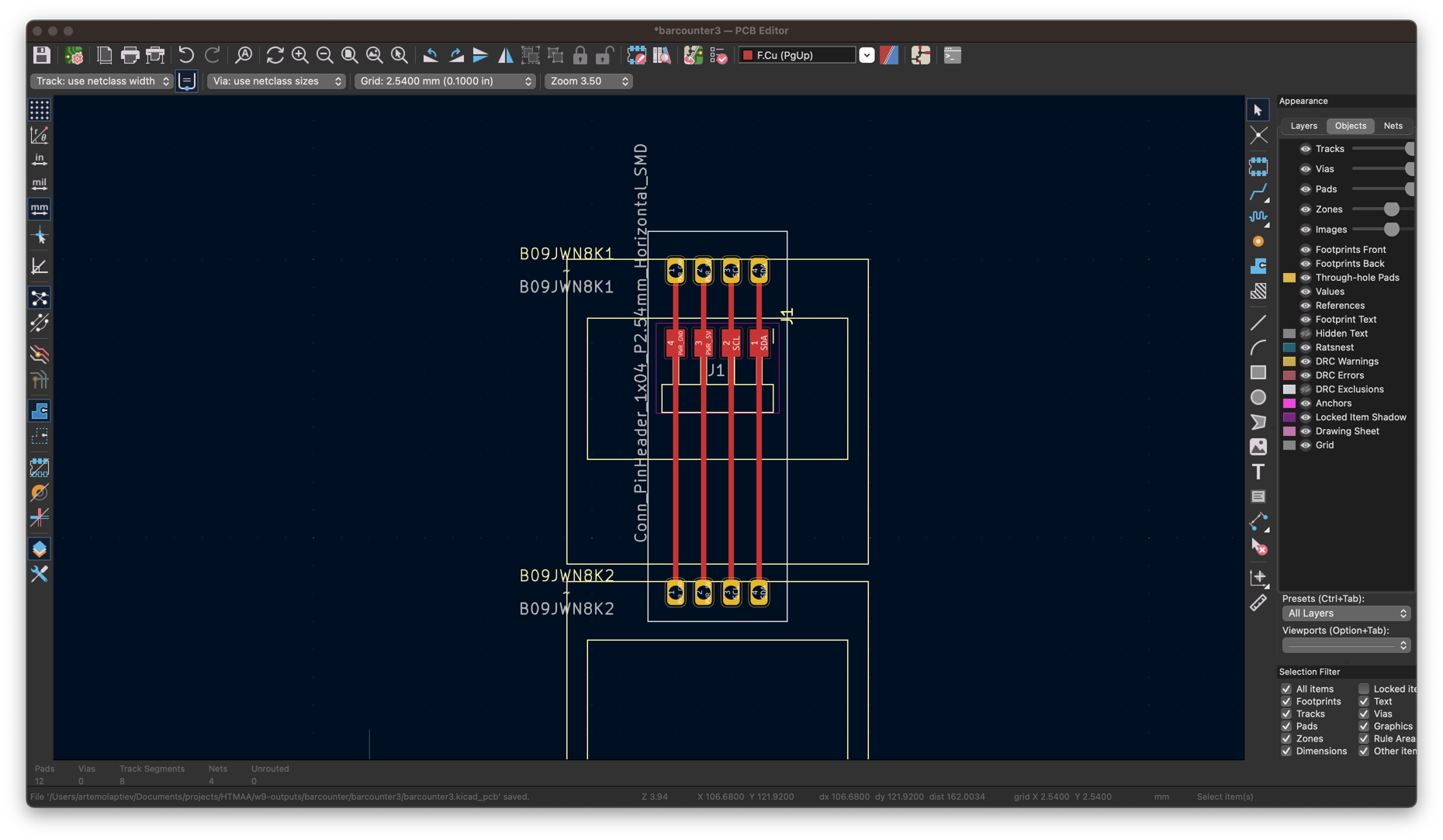
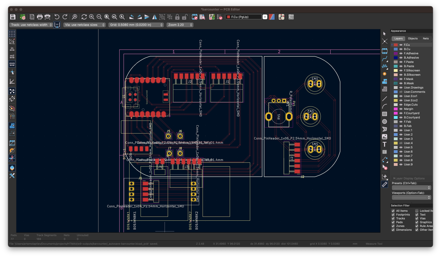
Full 3 boards:
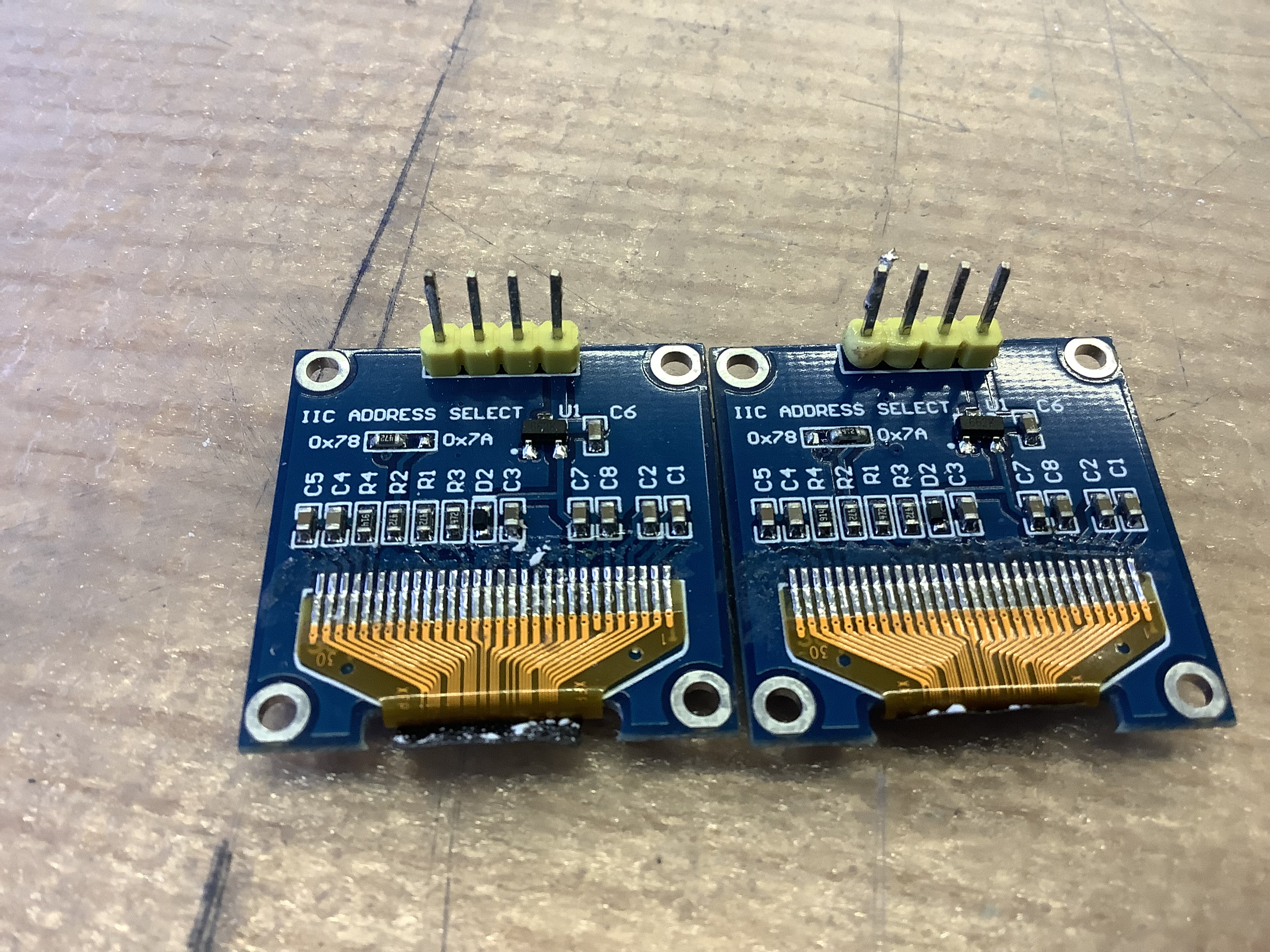
Two OLEDs I2C address clash. Have to rewire one of them to a different address:
Making holes:
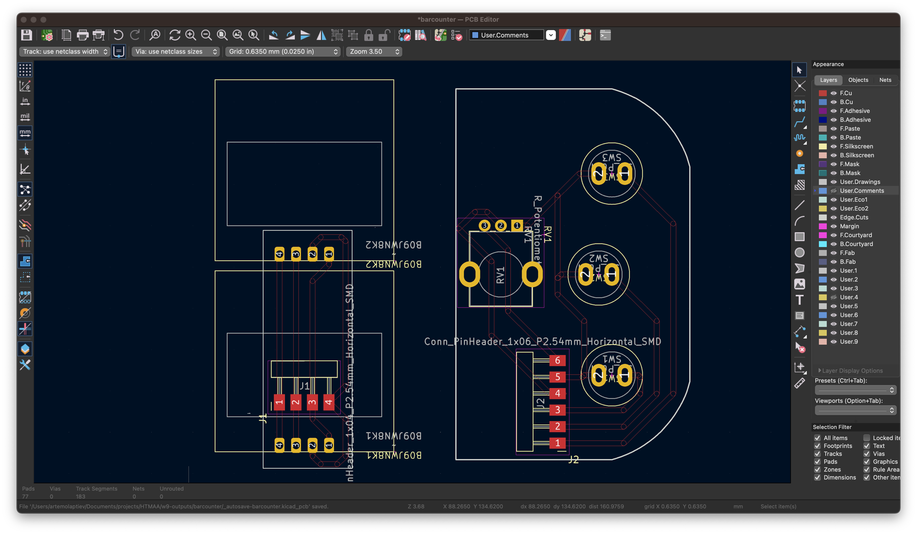
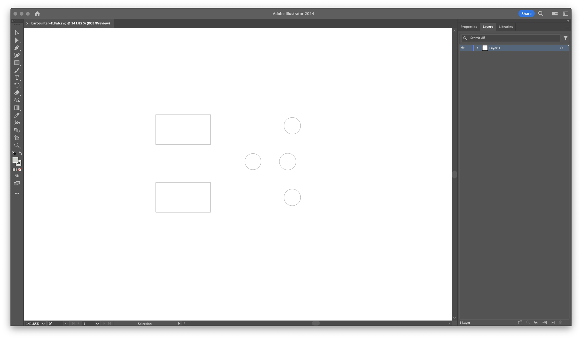
F.Fab Layer:
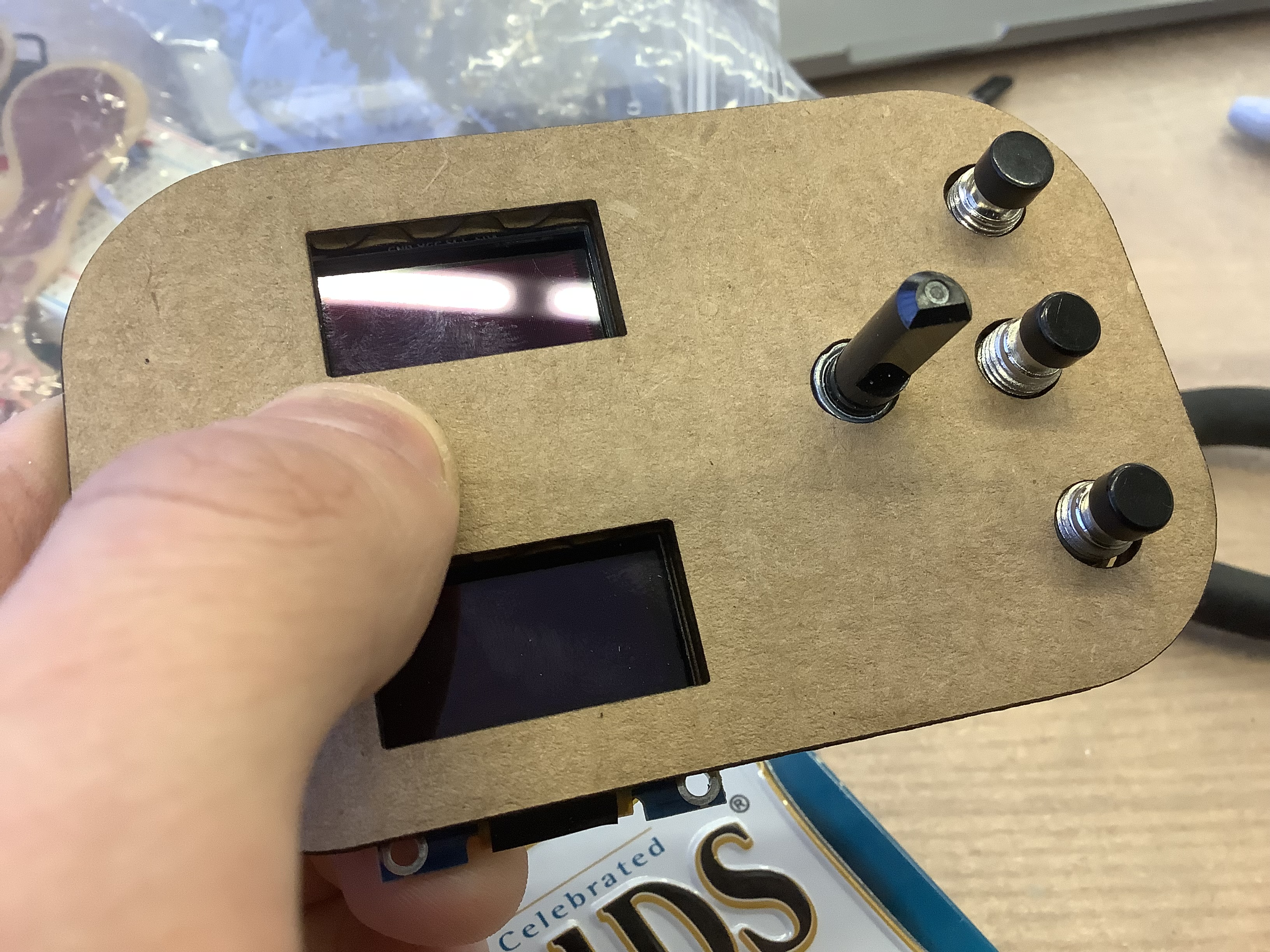
Print out last PCB + solder
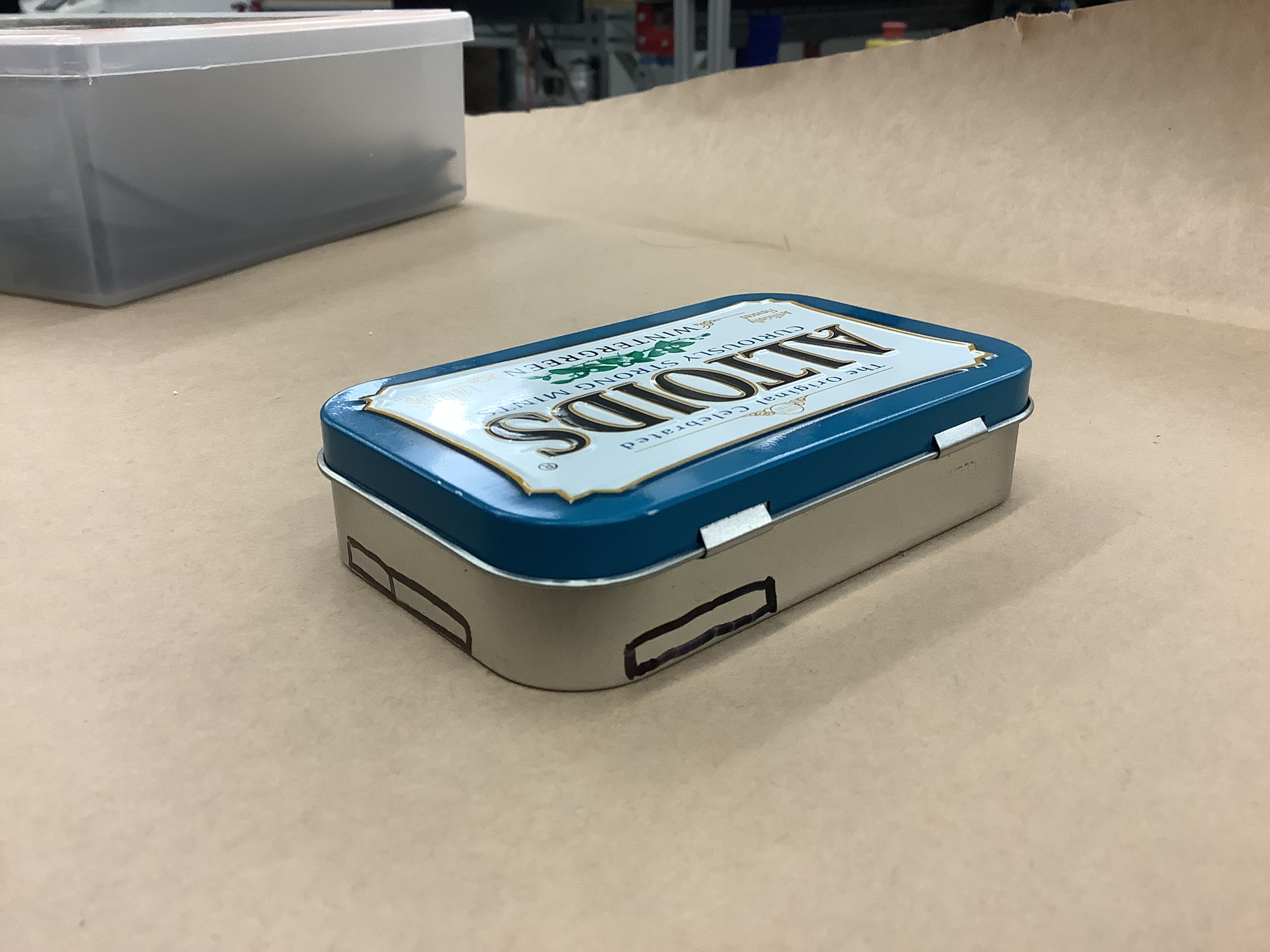
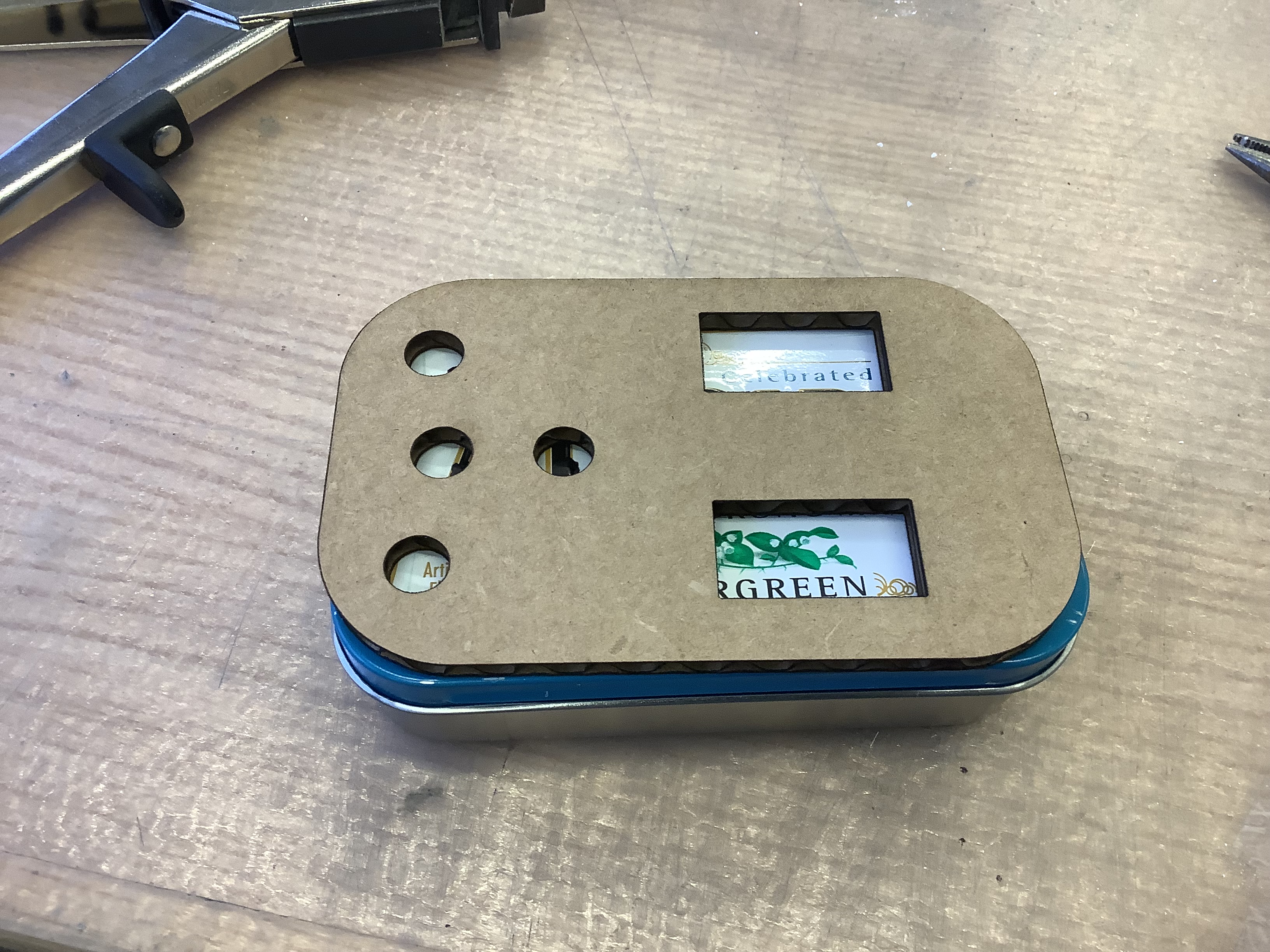
Try to fit into box

I2C Changing Address:
Laser cut new cardboard