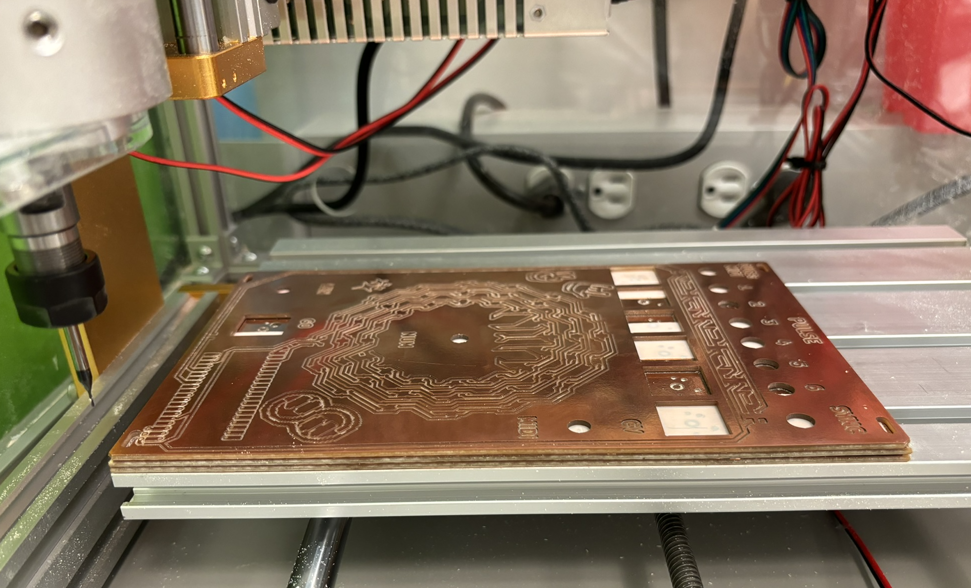
Tutorial: PCB milling
I wrote this quick tutorial for me and others planning to use manual PCB milling machines in the EECS lab. I include tips and tricks along the way!
Make a test mini-run with all components and double-sided traces
- Plot gerbers:
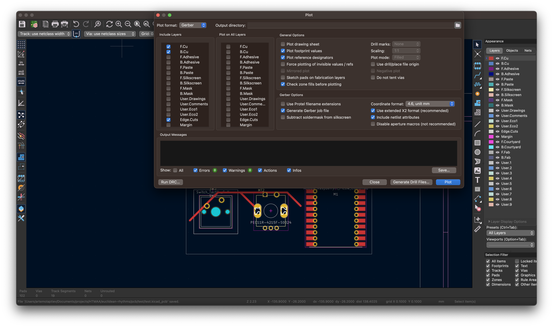
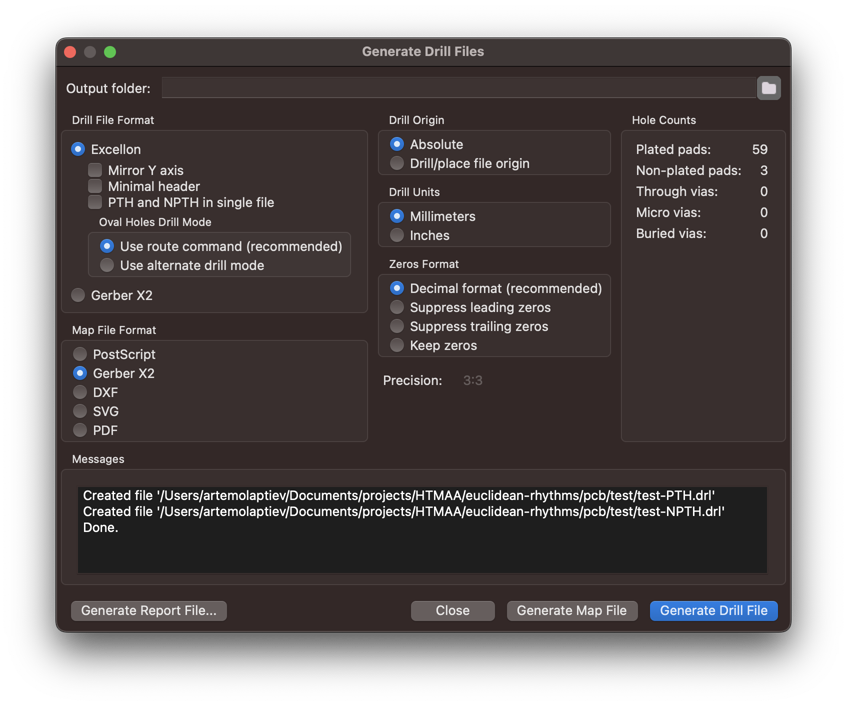
- Set Drill Units to Millimeters (!) and generate Drill Files
- Go to https://quentinbolsee.pages.cba.mit.edu/gerber2img/: Set Origin at x = - 0.025, y = - height + 0.025 Set Dimensions at x = width + 0.05, y = height + 0.05 Set Margins at 3 (or 0 for a full-size board, which is what I am doing) Render Black and White Render Fill edge cuts for edge only → For a board with dimensions 80.2mm x 70.3mm:
