Week 4 - How to Design (almost) any Circuit
This week, I thought of a new final project - rebuilding the Nintendo Gameboy - and I wanted to do something that would begin contributing towards the I/O of the device. I began by designing the circuit on paper, and while I was initially optimistic that using the Pico W would provide enough pins to manage the 8 buttons, the speaker and indicator LEDs, and the LCD screen, I quickly realized that I would need to use an additional chip to manage the LCD screen.
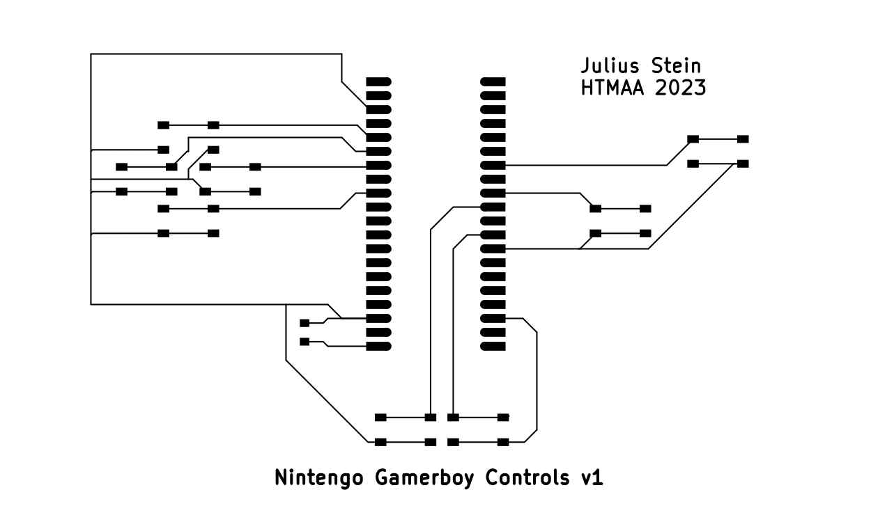
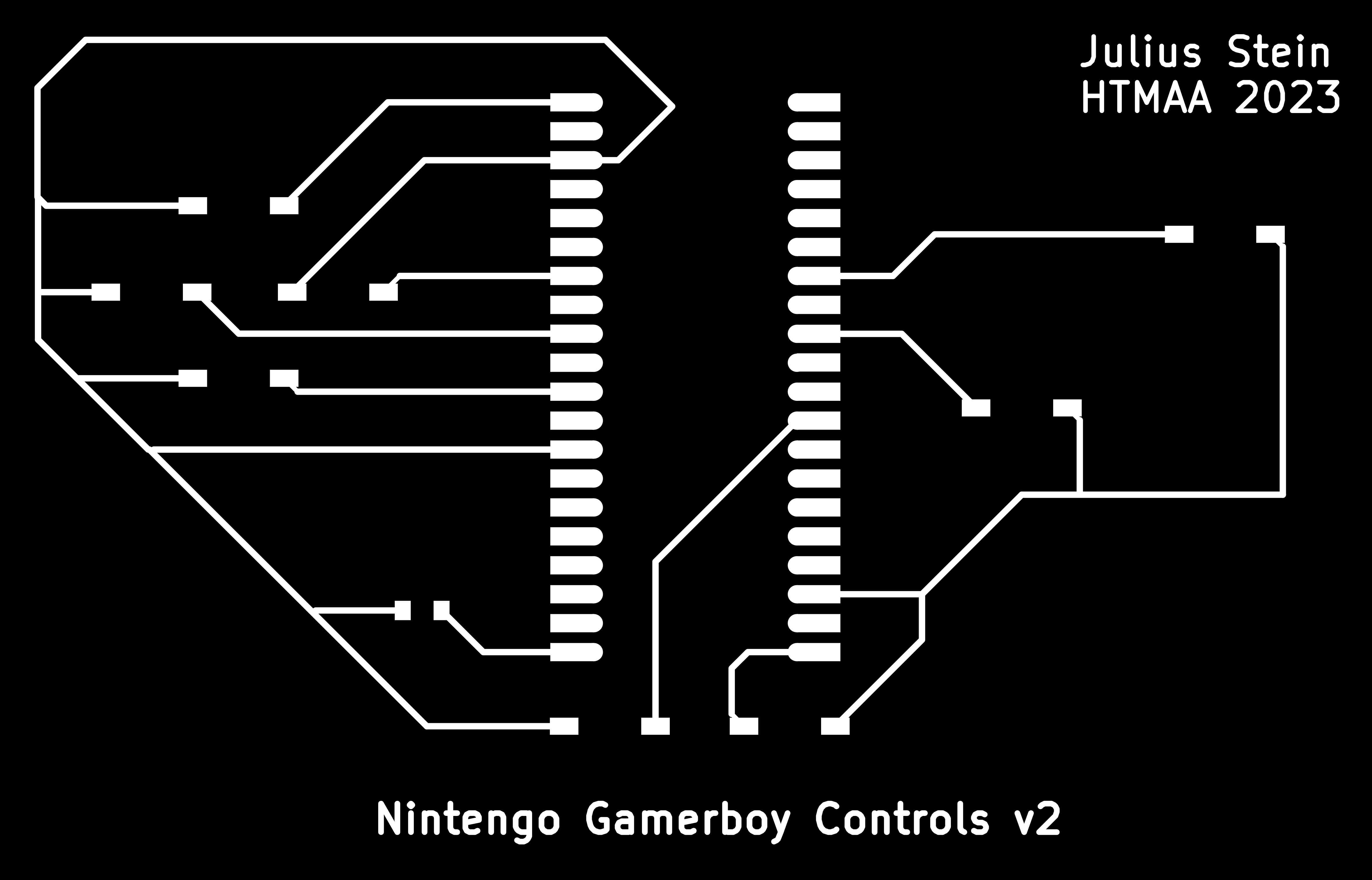
I then moved to KiCad to start designing the circuit for the controls and indicator LEDs. I began by designing the schematic which was relatively simple since each button or LED simply required a dedicated pin and a connection to ground. I then moved to the PCB layout, which was less simple. I was able to fit all of the components in the spacing that I believed would be sufficient for the final form factor, but when routing the traces, I quickly found that KiCad would not allow logical reordering of components on the PCB to allow for more efficient routing, so I found myself jumping back and forth to remap buttons to different pins so that routing would be more evenly distributed. I then drew a cassete shape for the outline of the PCB, added some text and exported the gerber files.
I first fouind that my minimum trace width was too small so I widened them. I then realized that I had used the wrong footprint for the buttons, so I replaced them, and since the new footprints only had 2 pins instead of 4, I was able to re-route all of the traces more simply. I then exported the new gerber files and moved to the CNC router.