Electronic Design
For the Electronic Design and Production Weeks I have set myself the lofty goal of making an electronic puzzle. My plan is to build a 3x3 puzzle where I can draw an image on my computer it will split the image into 9 equal chunks and then scramble them amongst the puzzle pieces. Each puzzle piece will be made of an OLED screen and an attiny 1624 chip. The base of the puzzle with have an esp32 xiao c3 will communicate with all of the puzzle pieces and learn their position.
Before I made the PCBS for the puzzle I wanted to test some quick prototypes to avoid making mistakes with electronics. So I thought a good first start was to make sure that I could communicate from the esp32 xiao to the attiny 1624 and then communicate from the attiny 1624 to the SSD1306 OLED Display
Above is a video of the esp32 xiao sending a message to the attiny 1624 to turn on and off the display, and then the attiny then sends a command to the screen to turn on or off (all of this communication happens over i2c). However, the attiny only has one i2c bus, so how does this work. The answer is software i2c (as suggested by Anthony). I was able to emulate a i2c bus over software using the Softwire Library and then I just had to make a slight modification to the Tiny4kOLED , the library I was using to drive the OLED, to support the software i2c. Then I keep the save the hardware i2c bus to communicate from the attiny to the esp xiao
This set up showed me that I need pullup resistors for all of the i2c lines, as well as I can not power each puzzle piece will a coin battery because it cannot produce enough current to power the attiny and the screen. So I will need to use a tiny lipo battery which means I will need the circuitry to charge the lipo as well as a 3.3V regulator to regulate the power
Also the width and height must be smaller than the oled screen (which means the PCB must be smaller than ~28 x 28mm). Because of the constraints on the width and the length, I thought it would be best to make this two pcbs that would then attached together
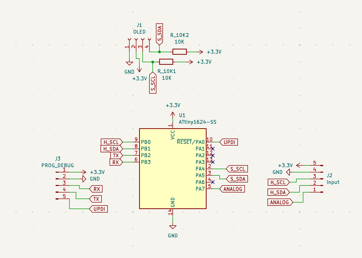
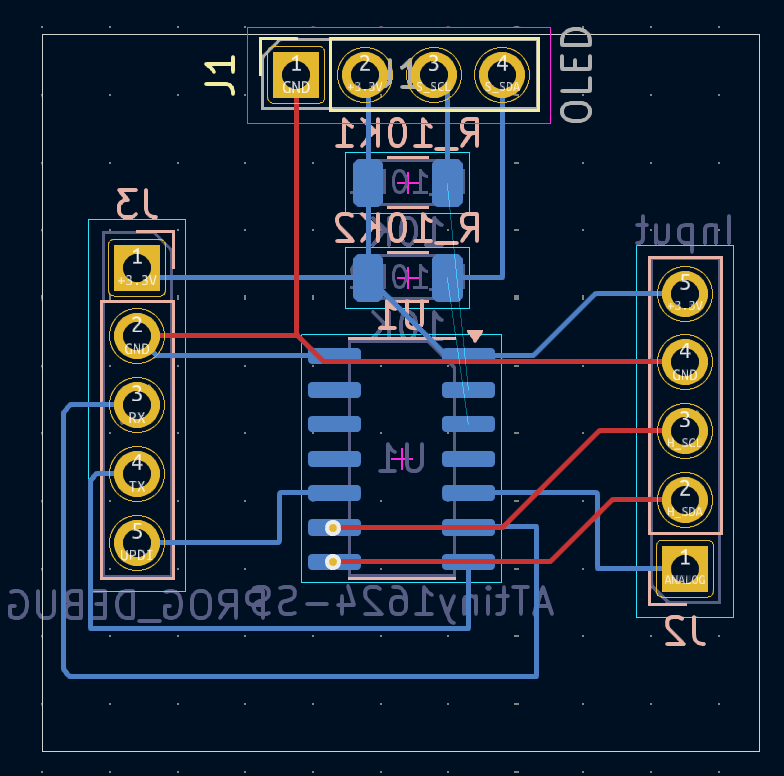
PCB 1: Attiny and OLED screen


The first PCB has pins to allow for programming and serial debugging, as well as pins to connect it to the secondary pcb, and finally sockets for the OLED screen to plug into
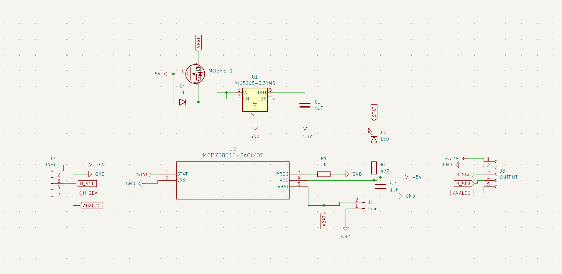
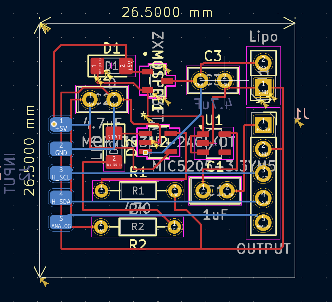
PCB 2: Battery Charger


The second PCB has sockets to connect to the first PCB, it contains all the circuitry for charging the battery and as well as a 3.3V voltage regulator, as well as copper pads which will be where the pogo pins on the base pcb which will is how the xiao will communicate with the attiny
Group Assignment
For the group assignment Jake showed us the oscilloscope, and we used it to analyze both a PWM signal and Serial Communication. We went over triggering to stabalize the waveform, we analyzed two waveforms at once, we looked at single trigger to stop the waveform the first time a pulse hits the trigger line, we used cursors to get more detailed measurements of our waveform, we also looked at the measurements menu to get live measurements of our waveform.