Group Assignment
- Characterize the design rules for your in-house PCB production process
- Submit a PCB design to a board house

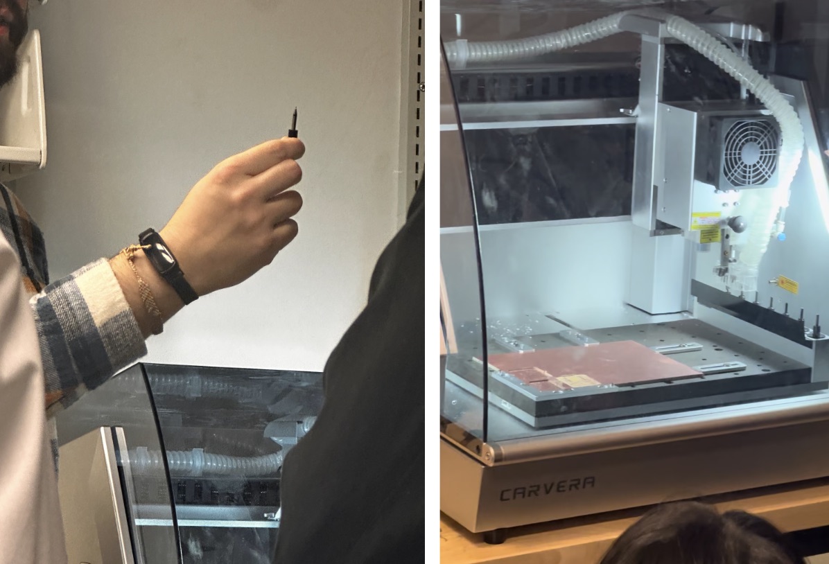
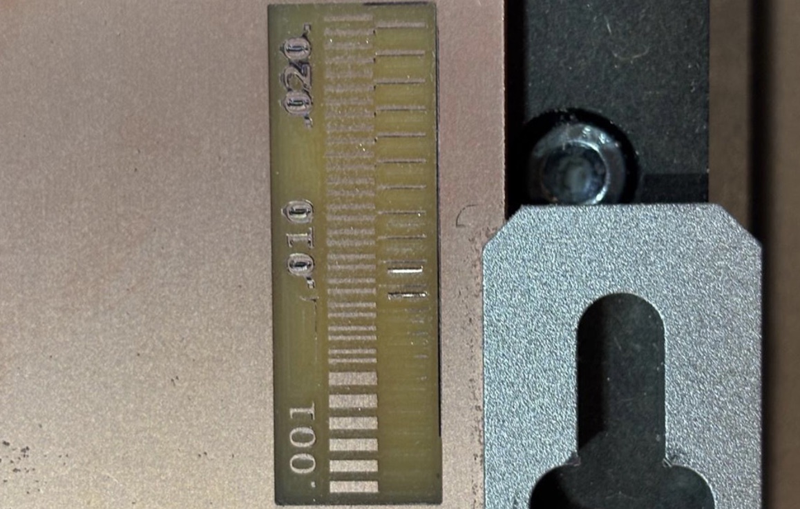
Our group met with Quentin, who guided us through the workflow for sending out a PCB for fabrication using JLPCB and discussed the different options available, including materials, solder masking, and stencils. He then demonstrated the use of the milling machine for in-house fabrication, showcasing a custom program he wrote to simplify the process even further; with this, we simply upload our files, and the program handles formatting. We milled this piece to test and review the machine’s design rules

More specifically, the recommended trace width was > 12 mils. Trace spacing minimum is 16 mils. Hole sizes need to be over 32 mils.
Procedure
Design the PCB
Use KiCad to design the desired PCB (e.g., using a 10k ohm resistor and Xiao RP2040).
Export Gerber Files
Once the design is complete in KiCad, go to File > Fabrication Outputs and export the design as Gerber files.
Convert to Black and White Render
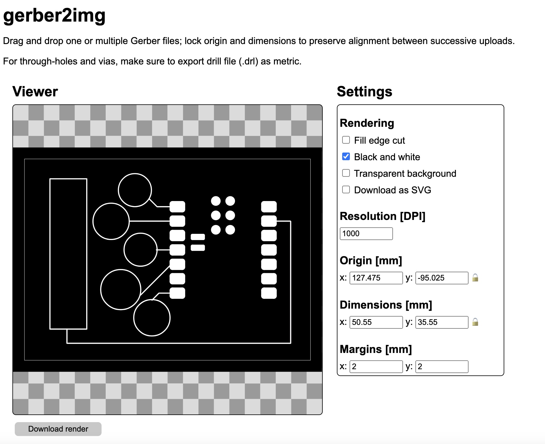
Import the F.Cu and Edge Cut layers into Quentin's Gerber2Img tool, select “black and white,” and export the render.

Generate G-Code
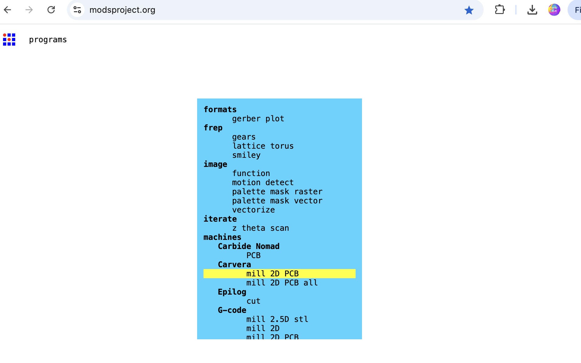
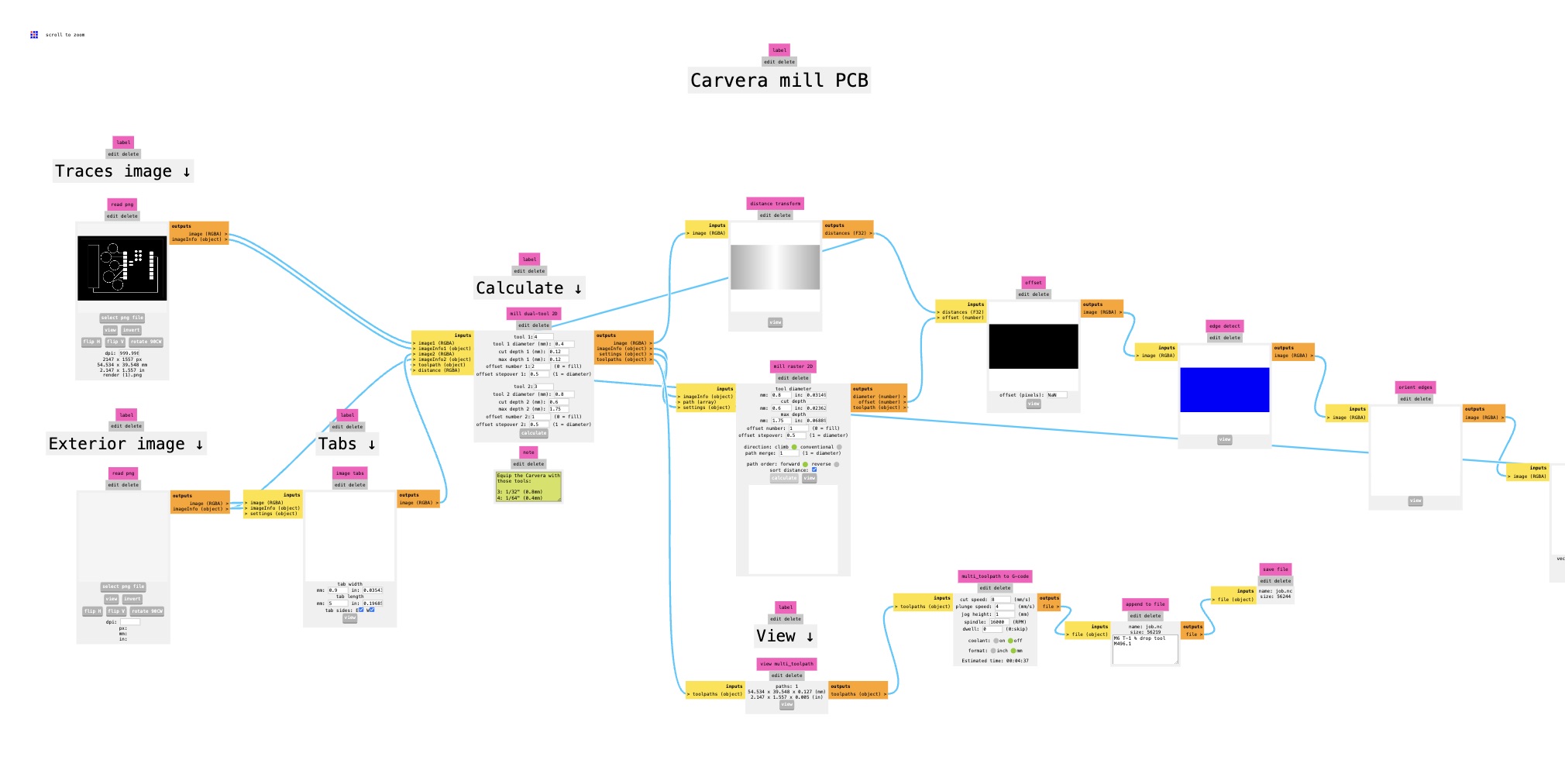
Import the downloaded PNG files into the MODS platform to convert them to G-code (use 1/64 for F.Cu and 1/32 for edge cuts).


Prepare CNC Machine
Import the F.Cu G-Code file to the desktop connected to the CNC milling machine. Secure a sacrificial copper sheet (bottom) and the milling copper sheet (top) using clamps. Attach the 1/64 end mill, using the blue guide to set the correct bit depth.
Set CNC Coordinates and Zero Z-Axis
Move the bit to x=0, y=0, attach the ground lead to the probe, and zero the z-axis.
Run the Mill Trace
After setting the z-axis, remove the ground lead, place the plastic cover over the end mill, turn on the vacuum, and press play to begin the mill trace.
Mill the Outline
After the trace, turn off the vacuum, remove the plastic cover, and exchange the end mill for the 1/32. Upload the EdgeCuts G-Code file, and repeat the steps above to mill the outline.
Remove and Inspect the PCB
Once complete, turn off the vacuum, remove the plastic cover, snap the PCB from the copper sheet, and inspect to ensure a clean trace. If issues are found, adjust the design and repeat as needed.
Solder and Program the PCB
Solder the necessary components onto the board and confirm there are no shorts. Within Arduino IDE, program the phototransistor to report sensor values from light detection.
Connect and Validate
Connect the RP2040 to the laptop, load the desired program, and use the serial monitor to validate sensor values by adjusting light conditions.
