-

To continue gaining momentum on developing PCB's, I decided to use this week to advance the work I started on the LED Monitor in P03.
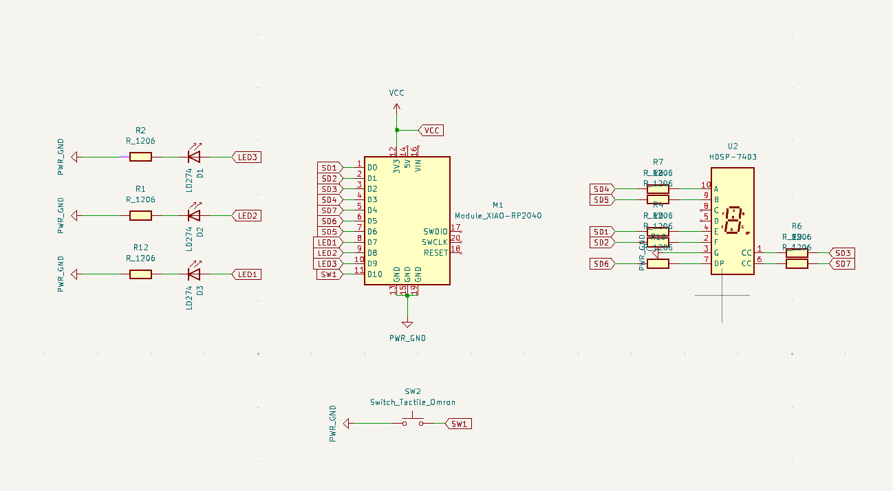
That meant i had to draw up a schematic for a PCB that utilized the RP2040 and included 3 LEDs, a button, and one 7-Segment Display.
For this i am using the software KiCAD. KiCAD has two viewing modes: Schematic and PCB Editor. I started by laying out the board logic
in the Schematic. Some important components to understand in this are:
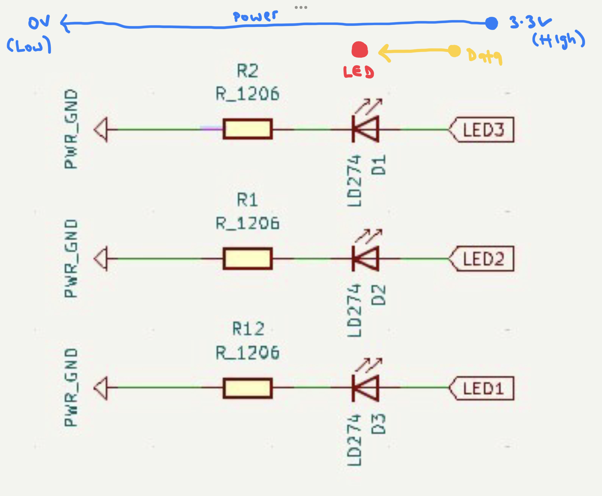
> How Power flows from microcontroller (or power source) to the components
> How Data flows from the microcontroller to the components.
-

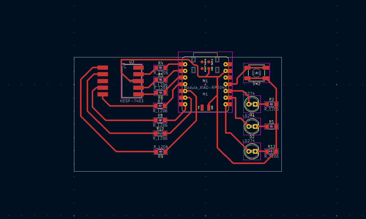
Once the Schematic is set up, you need to open the PCB editor to lay out the components and their traces. It's advisable to use thicker traces when
possible for easier milling down the line. I used 0.6mm. It's a fun maze routing the traces from the microcontroller to the componets, since they can't
cross. It's also generally advisable to leave enough clearing room between traces to avoid shorting connections.
PCB EDITOR
-

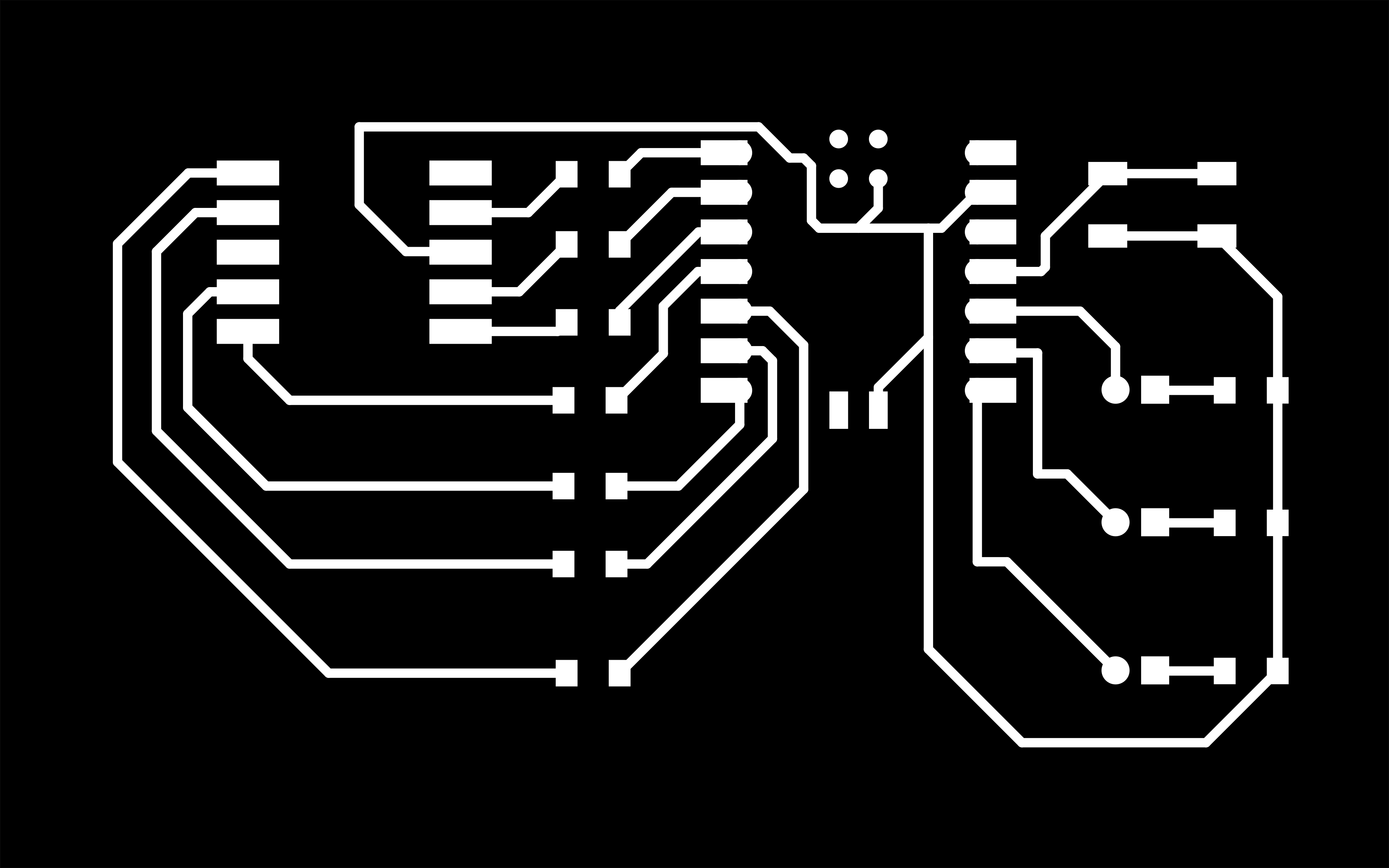
Once the PCB is laid out in KiCAD, you can "plot" the Traces and Outline as two separate PNG files. These are the files that will be used to mill the PCB.
-
