This week, I milled the PCB which I designed last week.
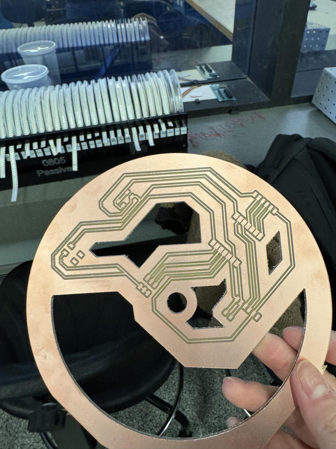
First, I had to scale down my PCB. I had intially designed it to be 20cm in diameter, which was bigger than the easily accessible boards in EDS, so I scaled my design down to a circle with diameter 15cm so that I could mill a 6x6 board. Since I had to adjust the routing slightly, I included the new board I milled, whcih you can see on the left.
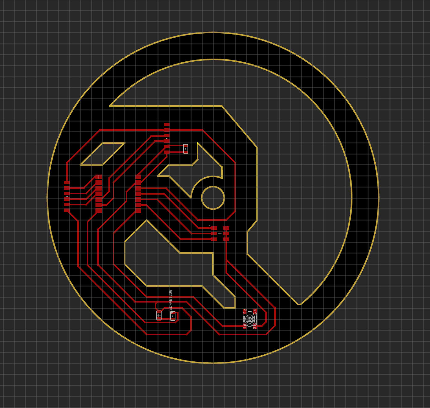
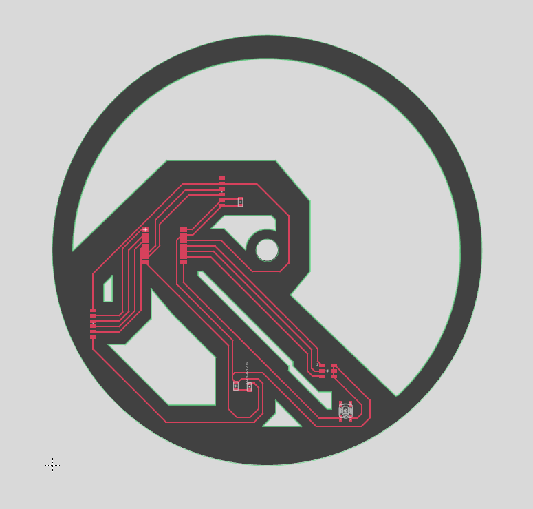
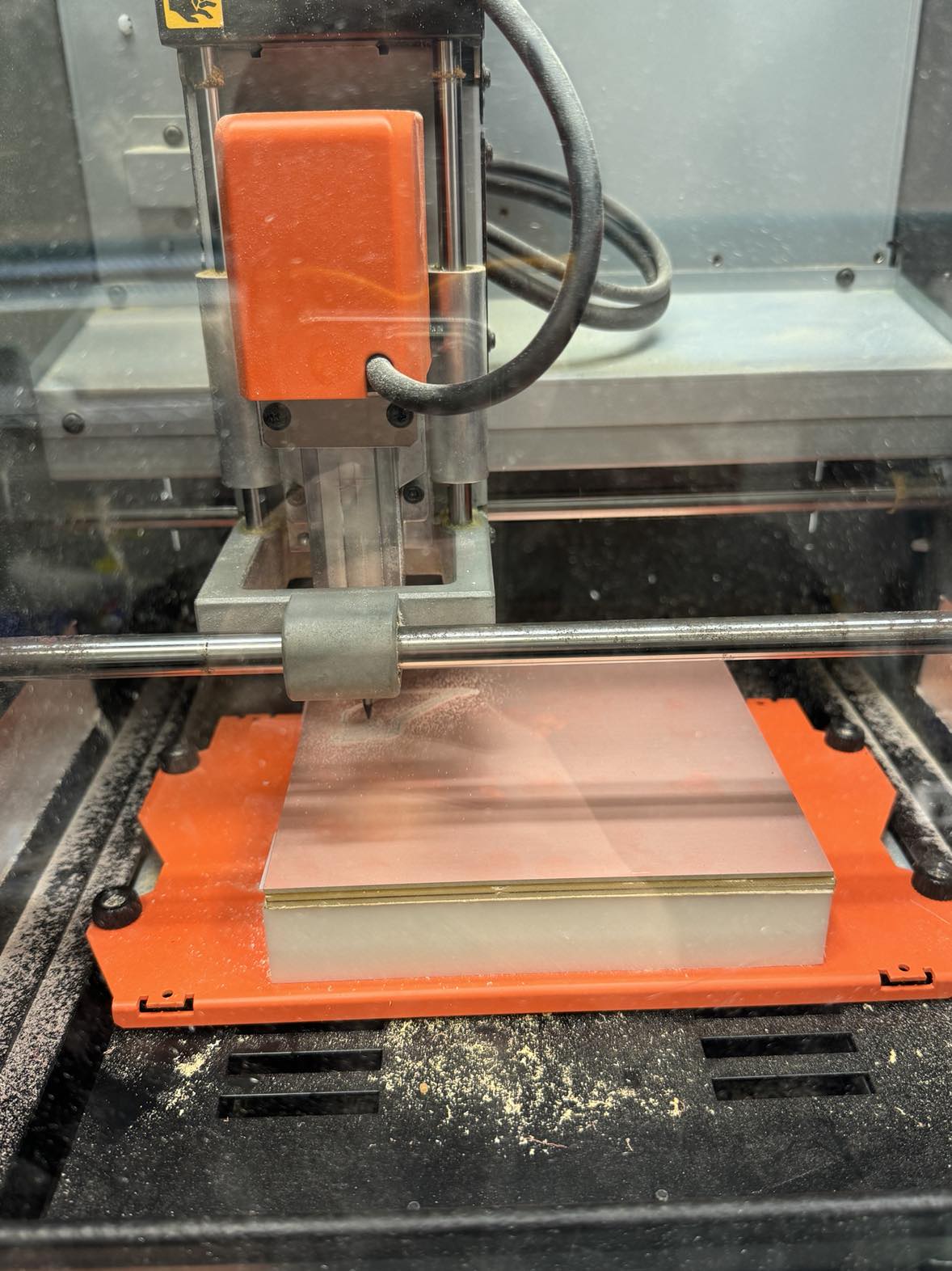

Once it was time to mill, Anthony taught me how to use the Roland SRM-20 instead of the OtherMill, since the SRM-20 can cut on 6x6 in boards. After a bit of set up with mods, you can see it cutting in progress here!
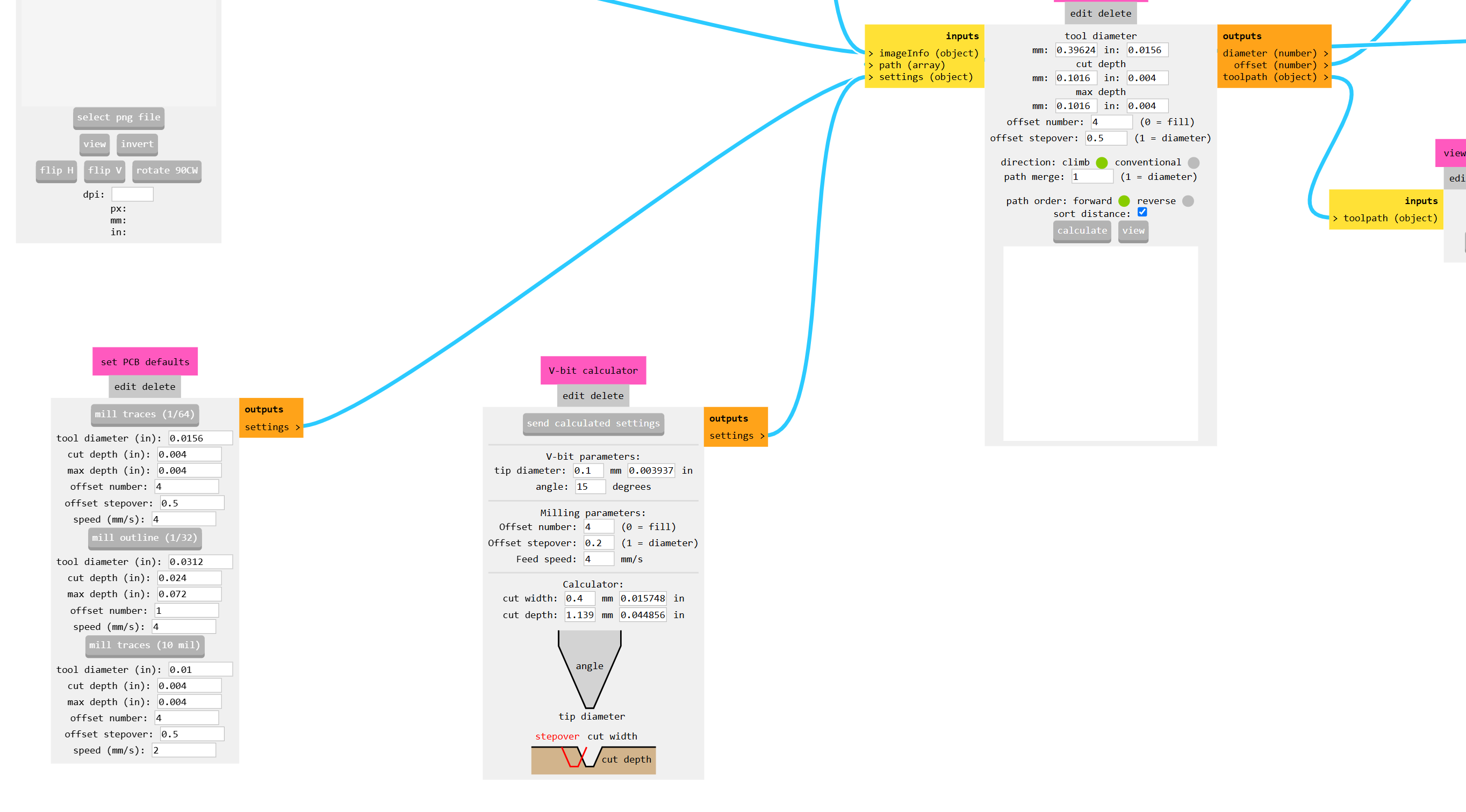
We went through mods, as well as Quenton's gerber2img site, where we exported the top profile and traces as gerber files that we convered to pngs. For the SRM-20, there are presets for milling traces with the 1/64th and board outline with the 1/32th. After uploading a png (note to self, mods cuts the black from the black-white boundry), we calculate the toolpath given the presets, then pair with the Roland and mill after calibrating the Z-height.
I ran into an issue during milling where the circle was slightly offset from the center of the board, so instead of cutting a perfect circle, the tool lifted at the edges where the design went off the board. Anthony taught me how to use a bandsaw so I could smooth out the rough edges that the lifting caused. I also messed up zero-ing the machine and ended up snapping a 1/32th" mill (or two), much to the dismay of the shop. Another issue was that I made a mistake in my mods set up (likely clicked something random, we were not able to figure out what it was) and the inital outline I tried to cut was too shallow, but also too deep to be a trace, making for not the neatest profile once I was able to cut it.
Once I did cut out the board, I lightly de-burred the top with fine-grit sand paper and a spackle knife for the edges.
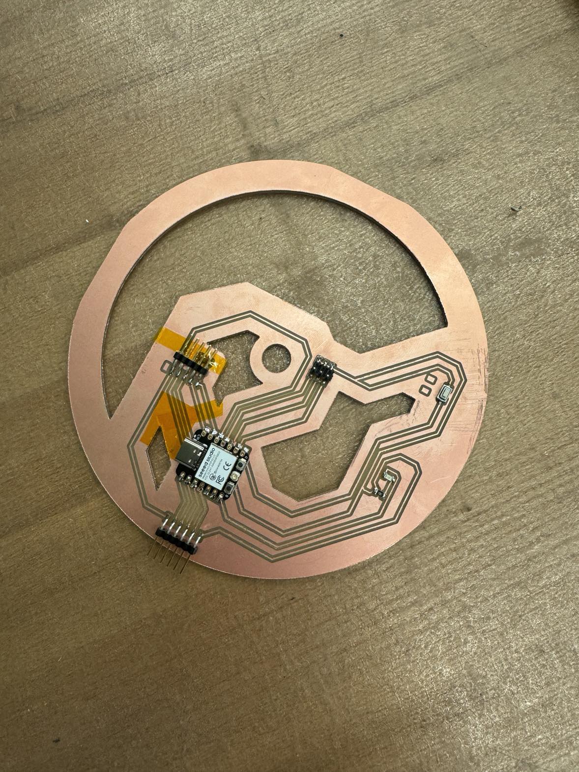
With a little soldering review and tips/tricks from Anthony, I added all my components!
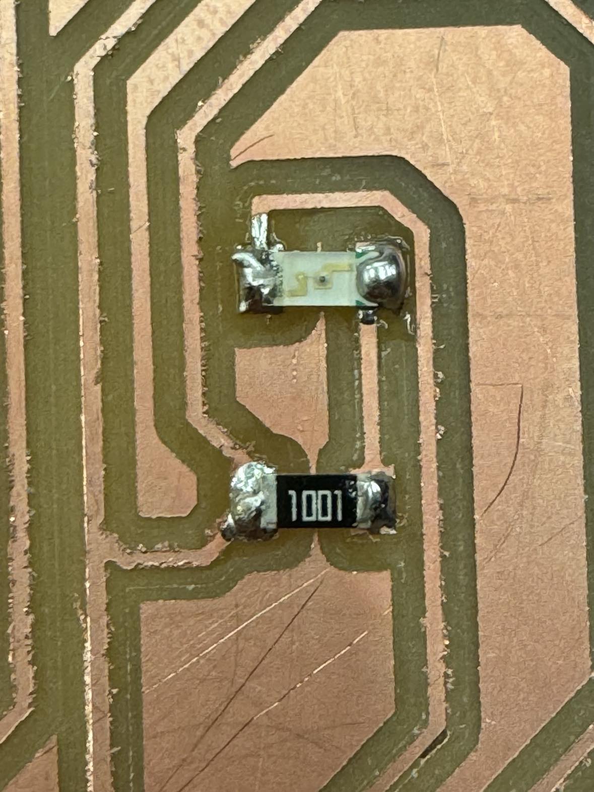
You can see a bit of the soldering work here in more detail. I also learned about polyimide tape, which I put on the back of my ESP32C3 so that the surfaces wouldn't accidentally lead to any trace jumping. I also added some near the USB-C port, since the USB-C cable head was made of metal and I had many traces there. You also can still see some burrs- most of the board was really elegant, but for the parts that were a bit messy, I can definitely improve my deburring skills.
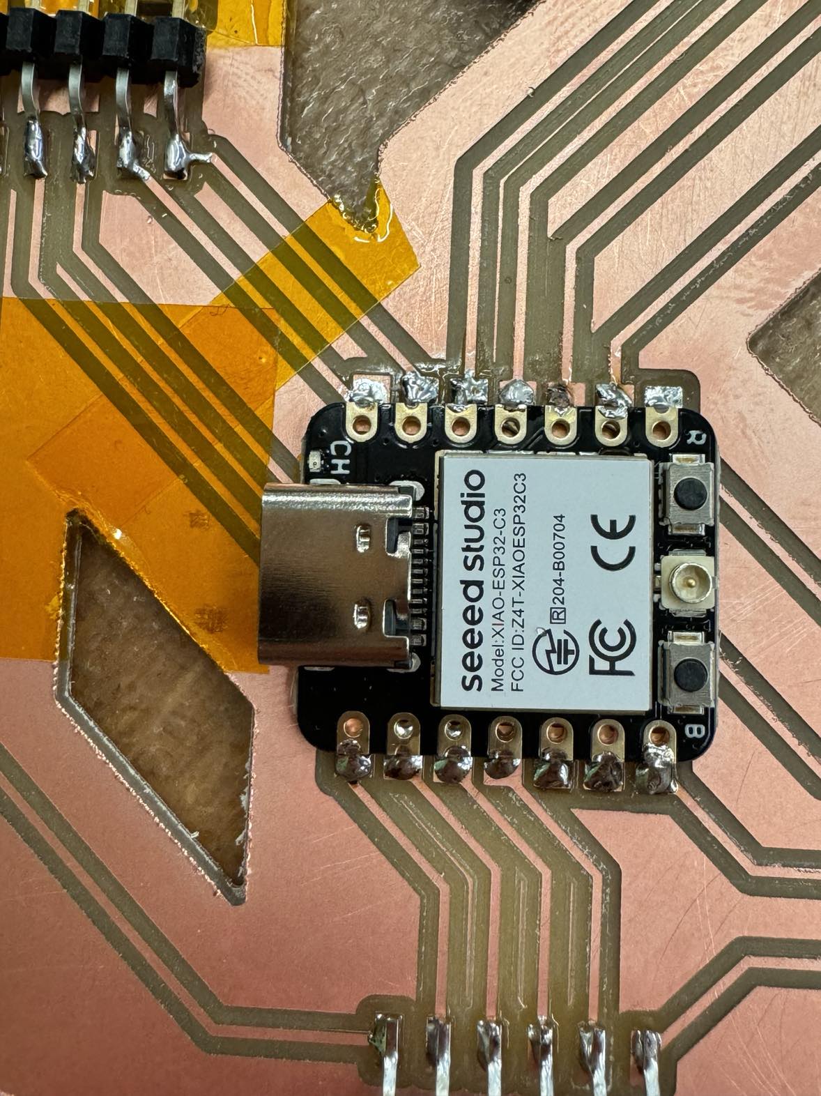
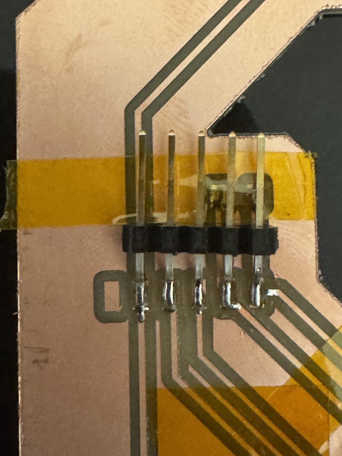
Making the board made some bad design choices very obvious. For one, it wouldbe easier to put the USB-C cable near an edge of the board so it doesn't block a bunch of components. Also, you can see here that I put a connector right next to a capacitor, which meant that once I soldered them both on, I couldn't actually connect anything to the two connectors above the capacitor since there was no space. I could've soldered it the other direction, but there was the USB-C cable there.
Once I finished everything, I connected the board to my laptop and uploaded the blink example, changing the pin number to the one I connected the external LED to, and voila!