HTMAA 2024 - Jonathan Cohen
For the group assignement the CBA section did a walk through with Quentin in the MARS lab. He gave us a tutorial on the use of test equipment to observe and debug electronics. We discussed the use of the basic EE toolbox scopes, multimeters and digital logic.
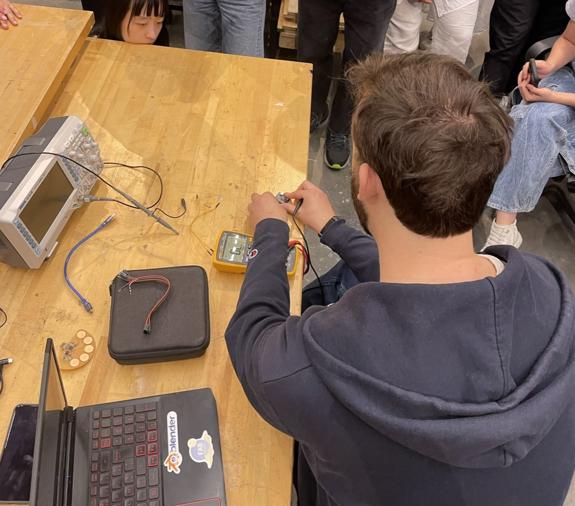
(Our section learning how to use the multimeter)
My goal this week was to design a basic dev board to drive future projects that require an mcu. I decided to go with the ESP32 so that I could interface with the board wirelessly. I chose fusion/eagle to design the board since I am so integrated with fusion now that I thought why not learn how to also make PCBs in fusion. Also, I love the idea of CAD software integrated with an EDA so I can have a nice workflow for enclosure designs!
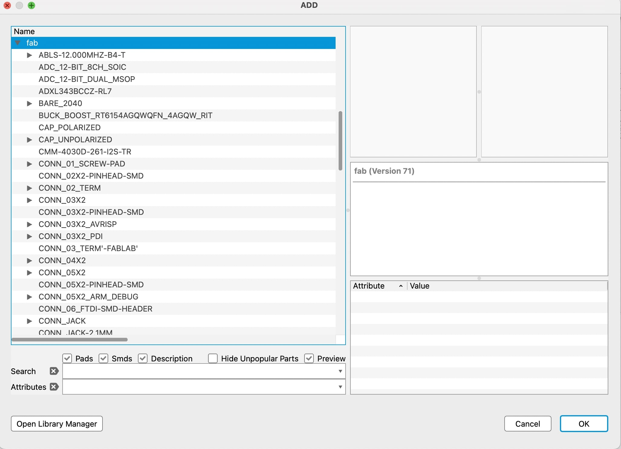
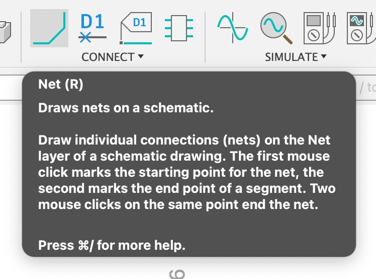
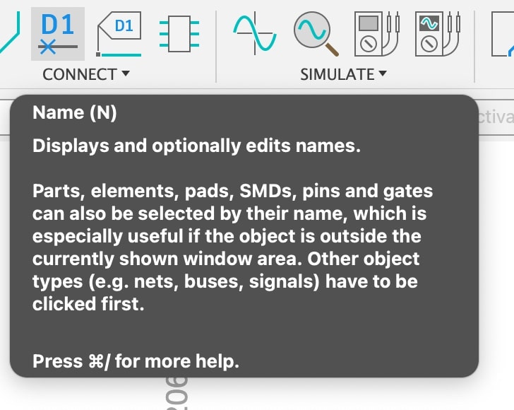
The workflow here is add a component --> Net (routing) --> Name (set value or connection). The software then pushes all of this wiring to the PCB view where we actually do the routing
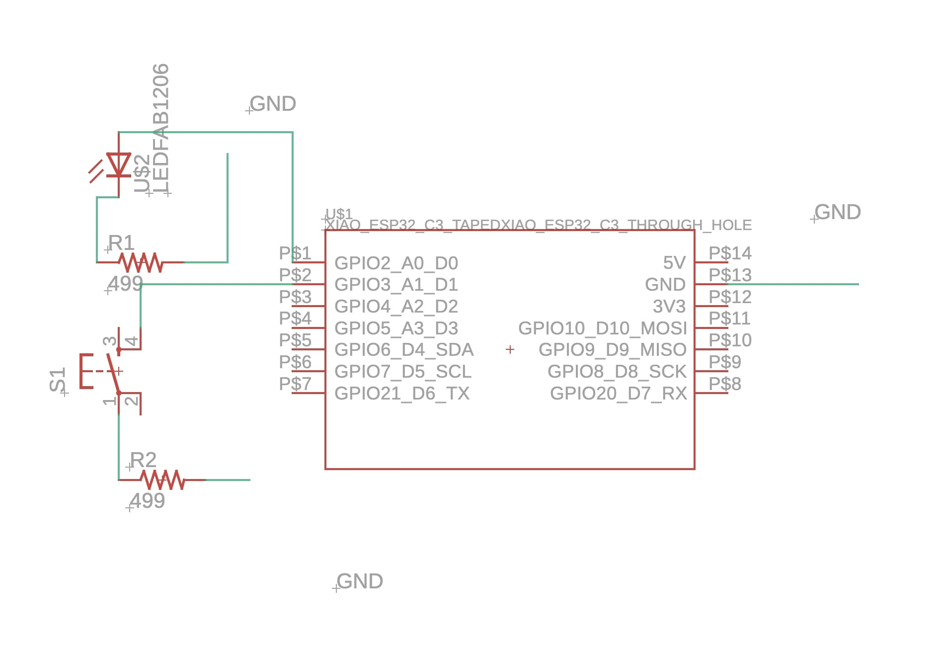
The schematic here is quite basic. The PS1 connected to the blinky LED and PS2 connected to a switch. We'll use the internal pull-up feature to make this function.
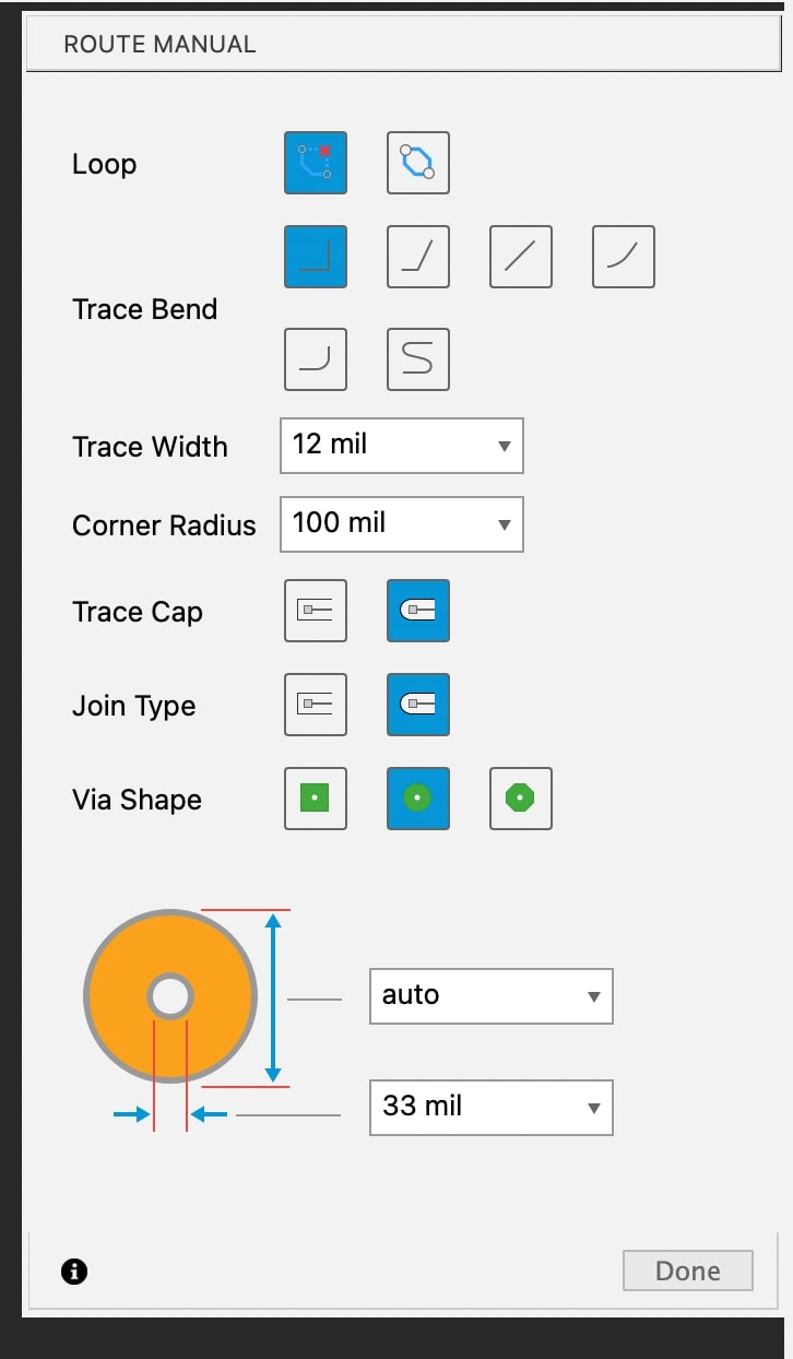
Route the board! Each time you click it will create a jog point
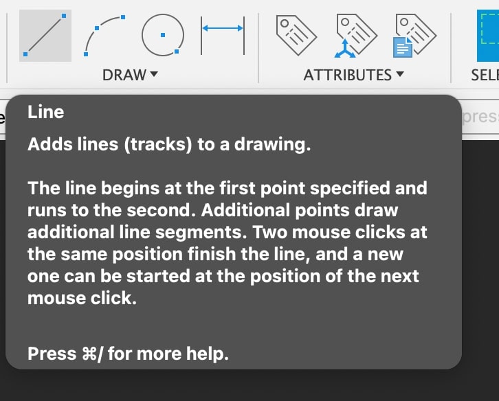
I used the draw tool to create a board outline and cut and drill a locating hole for a potential enclosure. I need to find out what tools the desktop mill has so I figure out the dimensions of the hole. I also would like to know what constraining techniques are ideal for this method of production.
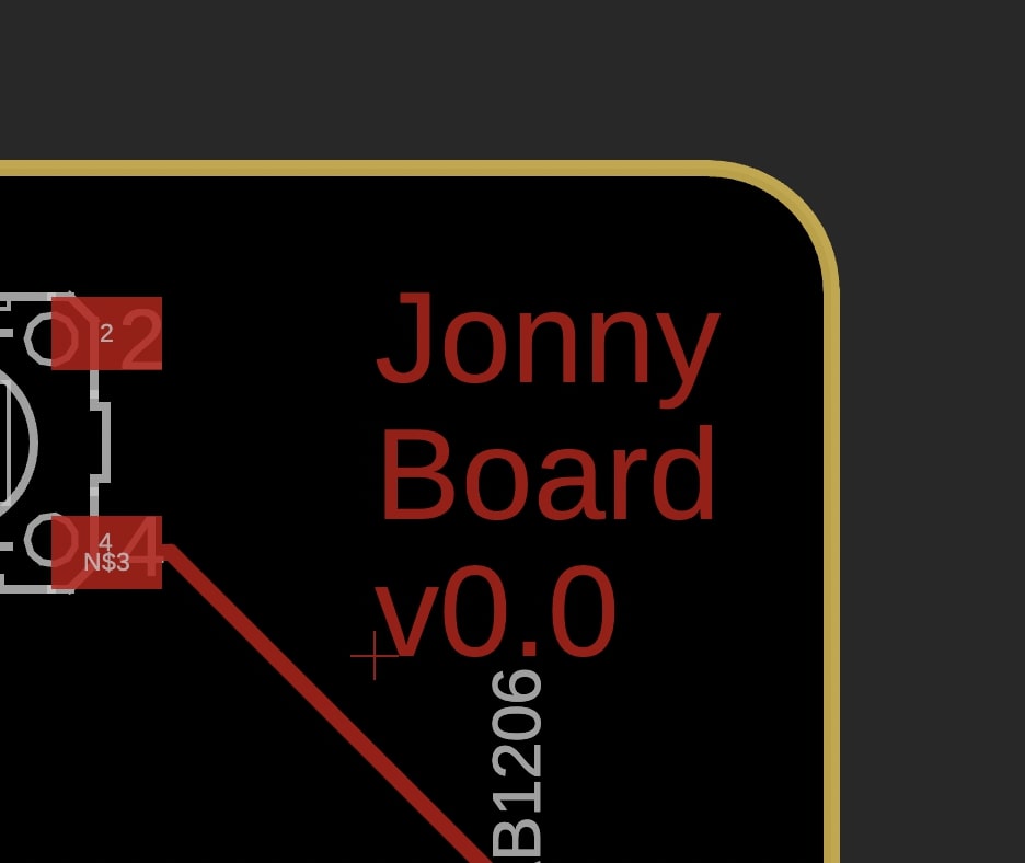
Using the text feature to name the board in the top layer so the mill will cut this text
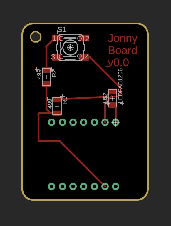
Here is the final design, simple but I learned how to use eagle! Although, I have worked on schematics and electrical designs before, I have never actually designed a pcb from start to finish so this was a very empowering unit! Big shoutout to Miana for helping me in office hours with this board and my questions about eagle. (CAD link)