Group Assignment: Test Equipment and Microcontroller Circuit
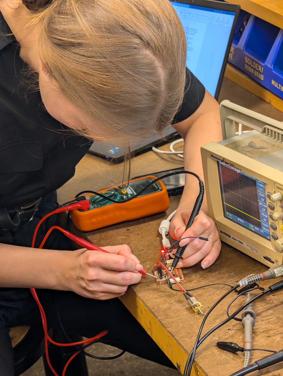
For the group assignment in the lab, we were instructed on how to use several key pieces of test equipment to observe the operation of a microcontroller circuit board. Our first task involved learning the functions and proper handling of a multimeter, which we used to measure the voltage, current, and resistance across different components of the circuit. This gave a clear understanding of how the microcontroller was powered and how current flowed through the system.
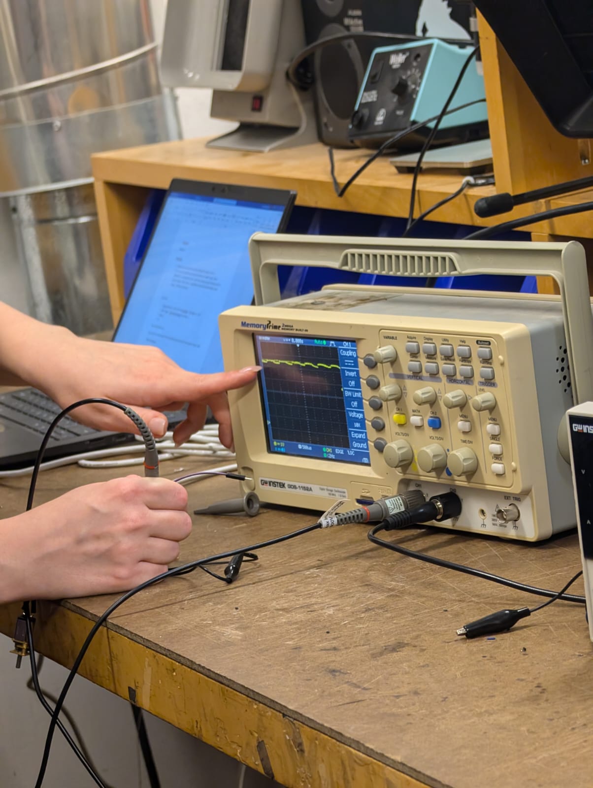
Next, we were introduced to the oscilloscope, an essential tool for visualizing the electrical signals in the circuit. With this, we were able to observe the behavior of the microcontroller's output signals, analyzing waveform patterns, pulse width, and frequency, which are critical for understanding how the microcontroller processes and controls external inputs and outputs. Lastly, we worked with a power supply unit to provide consistent voltage to the microcontroller, ensuring that we could vary the power levels and observe how the circuit responded to changes. By the end of the assignment, I was somewhat proficient in using these tools to diagnose and assess the performance of microcontroller circuits, reinforcing my knowledge of both the theory and practical aspects of embedded systems.
Schematic Design
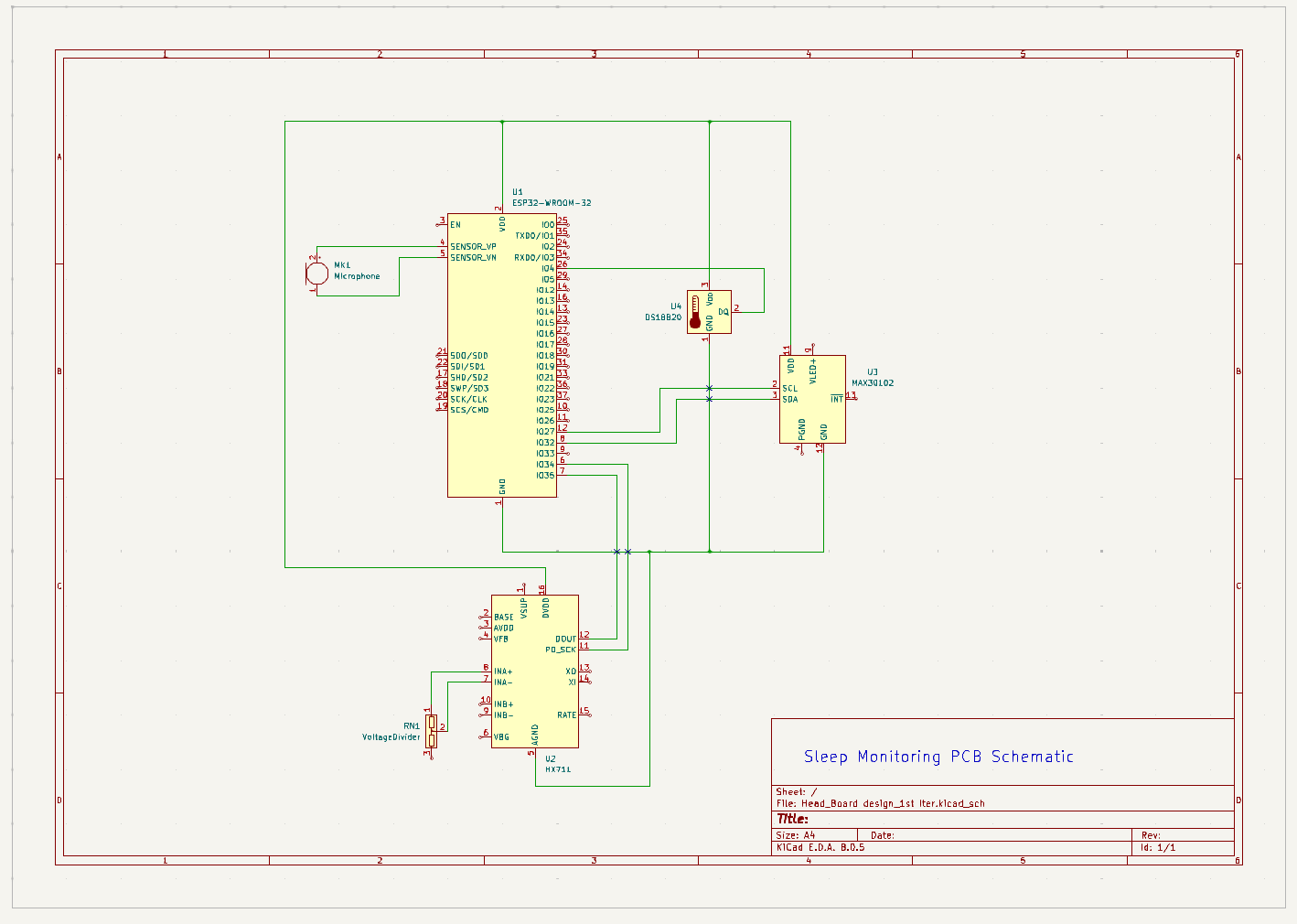
For this week, I started the EDA (Electronic Design Automation) process to design a conceptual PCB for a sleep monitoring headboard system using KiCAD. The system will incorporate sensors to track sleep patterns, snoring detection, heart rate, and temperature regulation. I selected the ESP32-WROOM-32 as the main processing unit due to its integrated Wi-Fi and Bluetooth capabilities and its ability to handle analog and digital inputs. The workflow began with the schematic design, moved to PCB layout, and ended with a 3D render of the board.
In the schematic stage, I selected key sensors for the system. Initially, I considered using TAL220 Load Cells for tracking body movement during sleep but later replaced them with a voltage divider as a placeholder. The HX711 amplifier was used to convert small signals from the voltage divider into data the ESP32 could read. For snoring detection, I used a generic Microphone from the KiCAD library instead of the INMP441(desired). The MAX30100 Pulse Oximeter was chosen to monitor heart rate and breathing, and the DS18B20 Temperature Sensor was added to track temperature changes. I made sure that each sensor had appropriate connections to the ESP32, with power and ground shared among components.
PCB Design and Layout
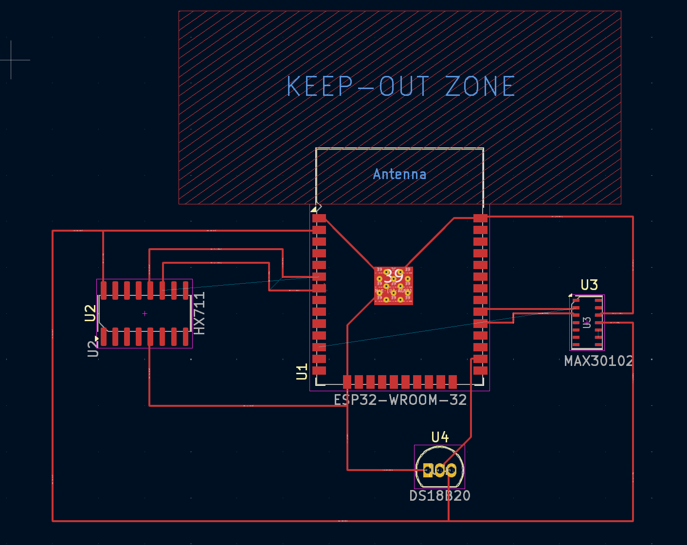
One of the key tasks was ensuring proper pin assignments on the ESP32-WROOM-32. I configured several GPIO pins for analog and digital inputs. To prevent wire crossings in the PCB layout, I had to modify the specific pin connections from the schematic. For example, I connected the HX711 amplifier's DOUT pin to GPIO12 and its SCK pin to GPIO11. The MAX30102 Pulse Oximeter was connected to GPIO10 and GPIO13 for SCL and SDA, while the DS18B20 Temperature Sensor was connected to GPIO7. The microphone was connected to GPIO4. These changes ensured a clean layout with no crossing of signal traces.
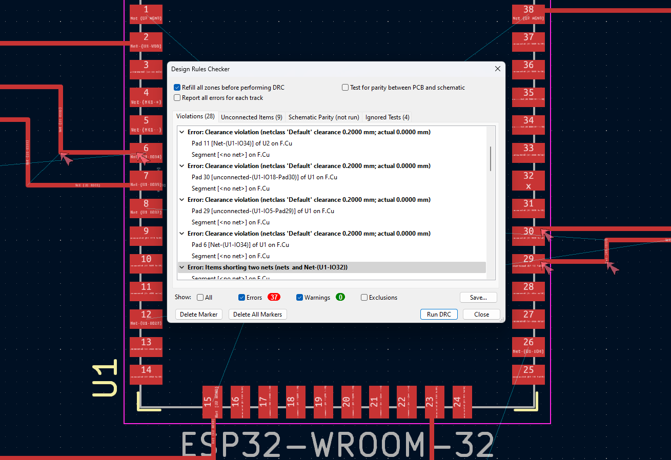
After completing the schematic, I moved on to the PCB editor in KiCAD. Importing the netlist, I positioned components to minimize crossings and ensure efficient routing. Some issues came up during the layout process. I encountered wires crossing between the load cells and amplifier, which I resolved by adjusting the routing and swapping pin connections. The DRC flagged a few clearance violations, where traces and pads were too close. I fixed these by adjusting the trace positions to meet the 0.2000 mm clearance requirement. Another DRC warning indicated that the board outline was missing, which I addressed by manually drawing the outline on the Edge.Cuts layer.
Error Resolution
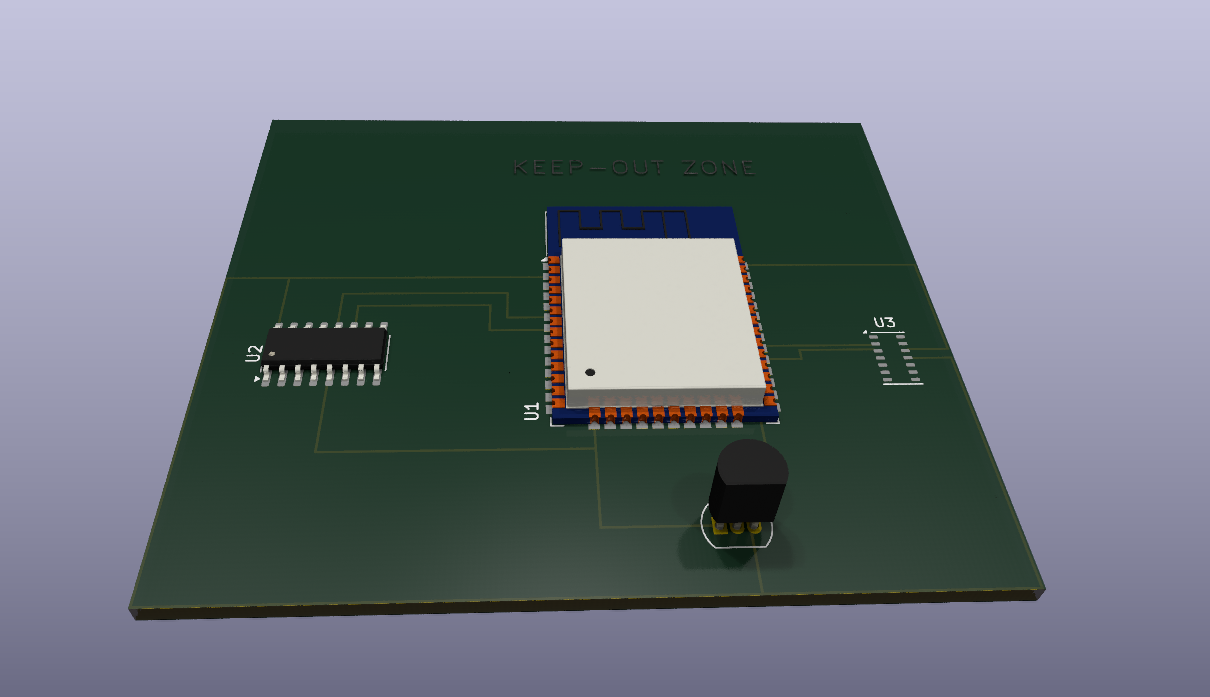
Once the layout was finalized, I generated a 3D render of the board. This allowed me to check the physical arrangement of components and ensure that the board would fit into the intended enclosure. The ESP32 module, the voltage divider placeholder, and other sensors were clearly visible. The render helped confirm that component placement and height were sufficient, and there were no clearance issues.
During the design process, I also resolved several errors flagged by the DRC. A short circuit was detected between two nets that I resolved by adjusting the routing. There were also some clearance violations that I corrected by rerouting traces. The missing board outline was resolved by manually adding the outline, and I optimized the overall layout by reviewing pin assignments and adjusting routing where necessary.
3D Rendering
I then rendered the board in 3d using the in-built 3D-View function and rendered it with ray-tracing
The next weeks will involve physically designing the board and checking if it fully covers the scope of the sleep monitoring project, ensuring all the sensor inputs are properly integrated and functional.
PCB Design Files
The following zip file contains the KiCAD project files for the PCB design, including the schematic, PCB layout, and associated design files. These files are useful for reviewing and physically prototyping the design.
Download Head Board PCB Design Files
