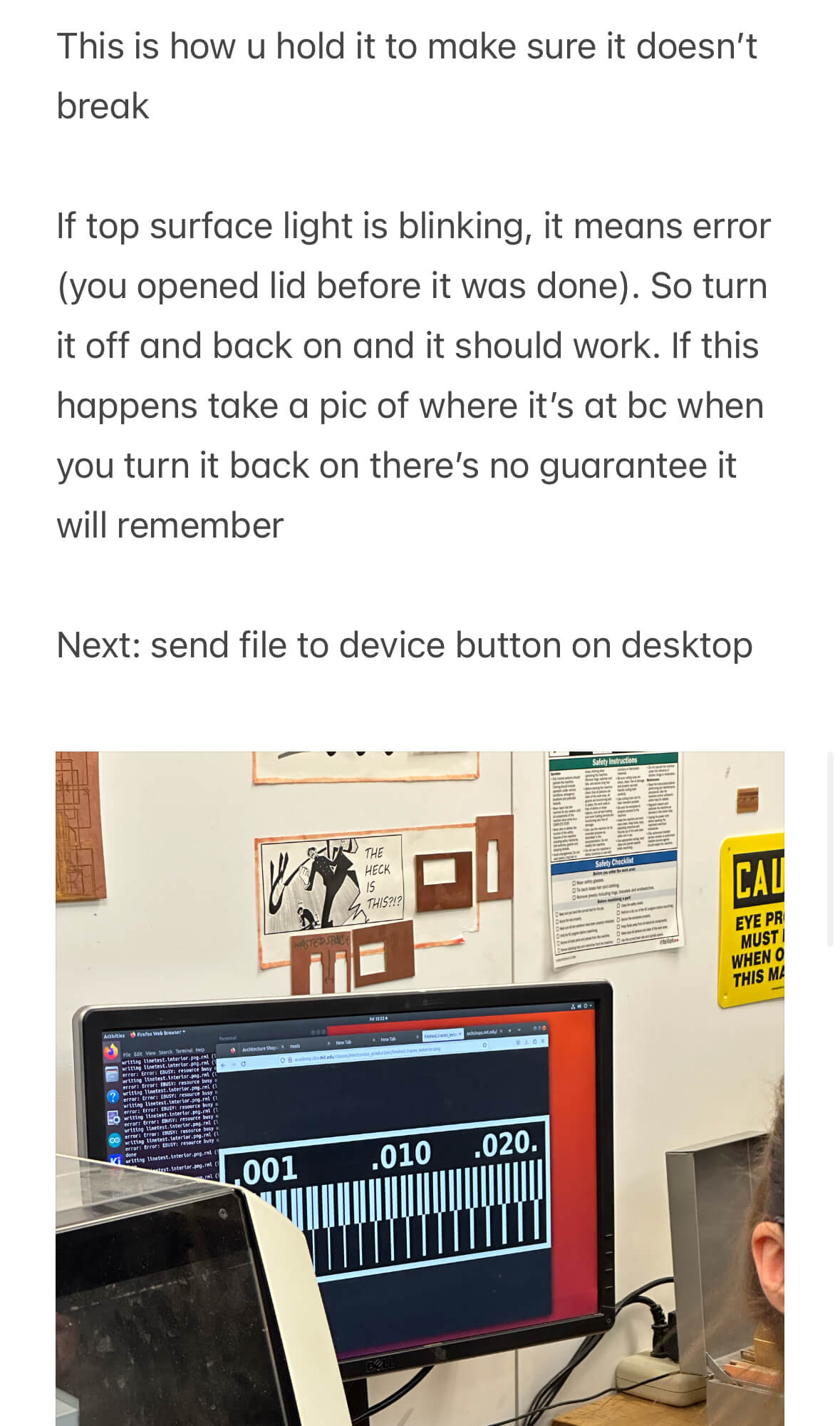
It's time to mill my pcb. I exported my pcb design in the gerber format, which resulted in two files: one for the traces and another for the edge cut. I then put them in Quentin's Gerber 2 image tool. Something weird was happening there. Even when I selected the Black & White option, it would export as a png with a transparent background.
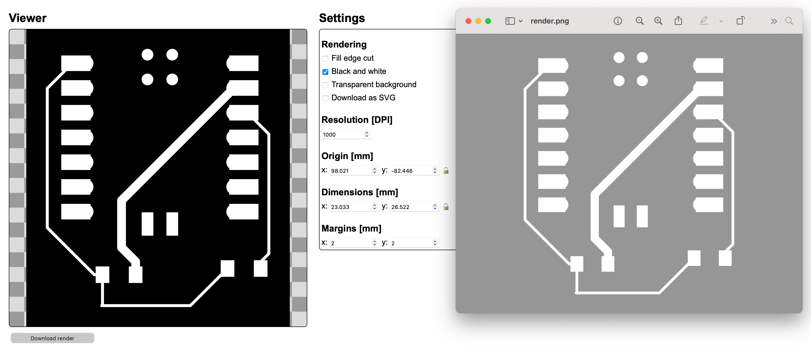
I was trying to figure this out with Diana and Javier, and we ended up just putting them in photoshop and adding a black background. We then put them in the system on the computer and milled them. Diana was amazing; she guided me through the process step by step and showed me how to do everything. Huge thank you!! There was actually a small problem with the machine. This is how my first mill looked like:
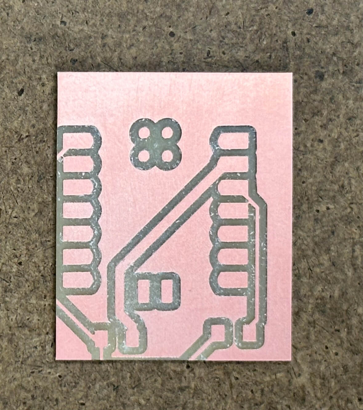
I initially thought it was a problem with my PNGs, given that we didn't use the originals. However, Diana said that it was probably the machine, because the same thing had also happened to someone else before. We went back to photoshop to make sure the traces and edge cut aligned properly, and they did, so we exported the two layers from the same photoshop file this time and tried milling again. It worked this time! It was still off-center, but it was something I could work with.
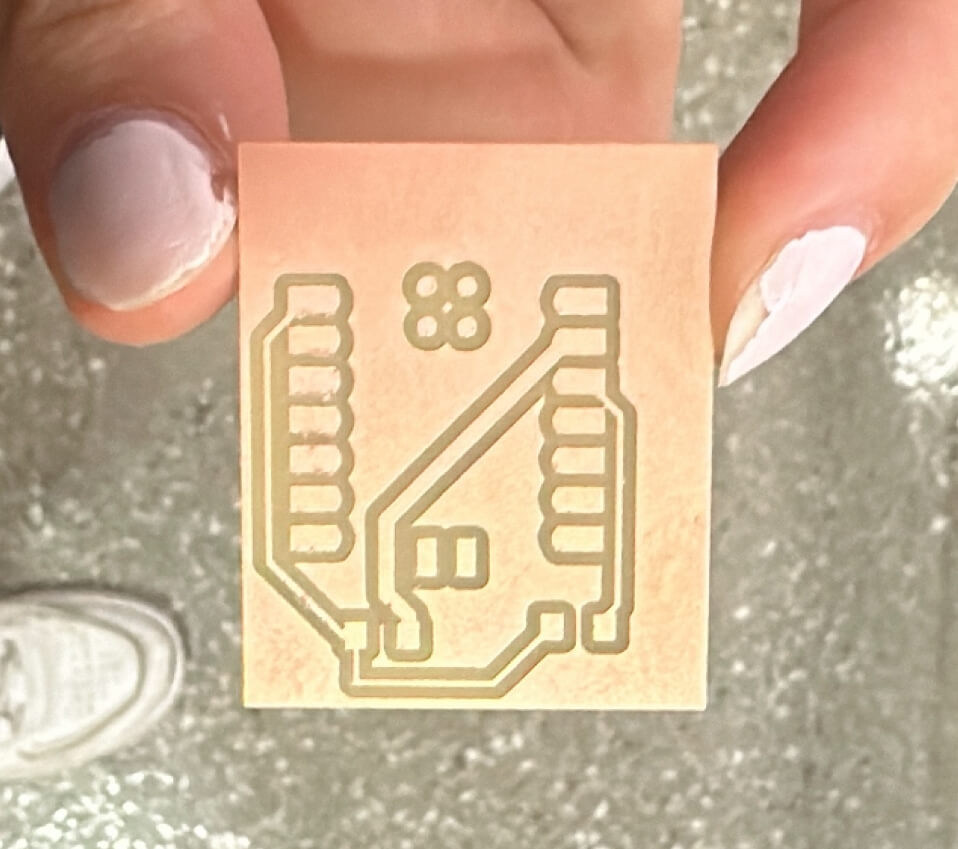
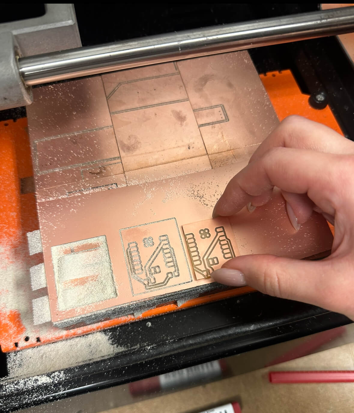
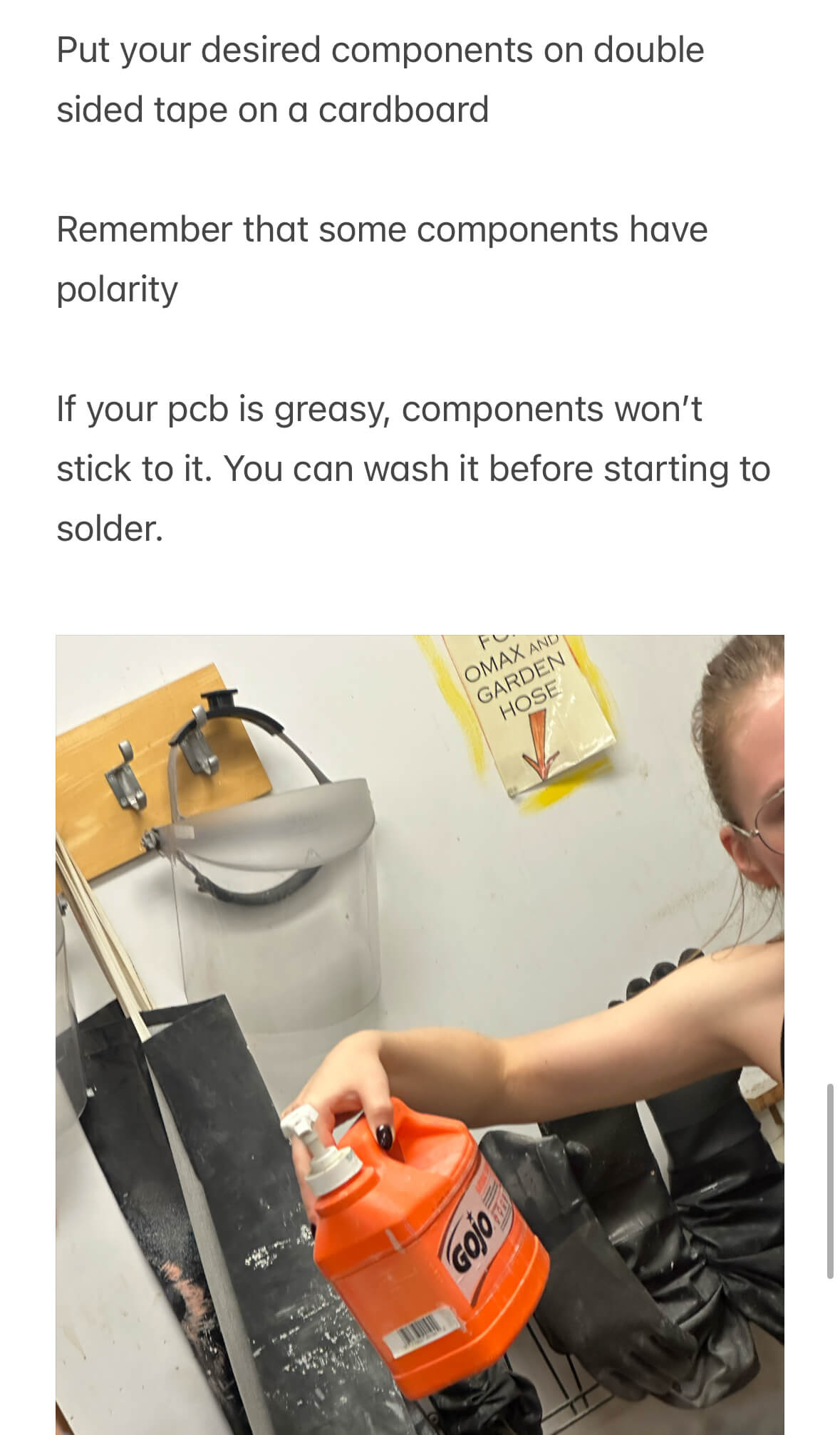
Now, I needed to solder my components. I cleaned my PCB with soap and water, and set to soldering. I used my PCB editor screenshot as a reference of what goes where, and taped all my components to a piece of chipboard.
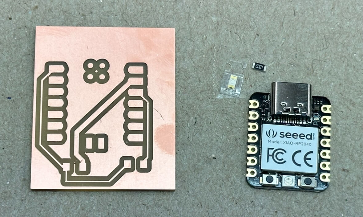
Even the microprocessor was moving a lot and sliding on the PCB when I first tried soldering it, so I taped it from the top to keep it in place. After the first couple of pins were soldered, I removed the tape because it was no longer needed. The resistor and transistor were tiny!! I had never worked with anything this small, and it felt like I was doing something super detailed when I used the tweezers to move them around.

To get those smaller parts soldered, I first put a small ball of solder on the PCB, and then used one hand to hold the soldering iron and another to hold the tweezers carrying the component. I melted the solder and then quickly put the component in it's position. Then, the second soldering point for that component was easy because the solder was already holding it in place. I had soldered a tiny bit before, in 4.031 (Design: Objects and Interactions), so it wasn't tooooo difficult or frustrating. That said, my work still started off pretty messy and got better as I went along.
The next thing to figure out was the polarity of the transistor. The data sheet had a diagram that showed it (Thank you to Alex for pointing that out!).
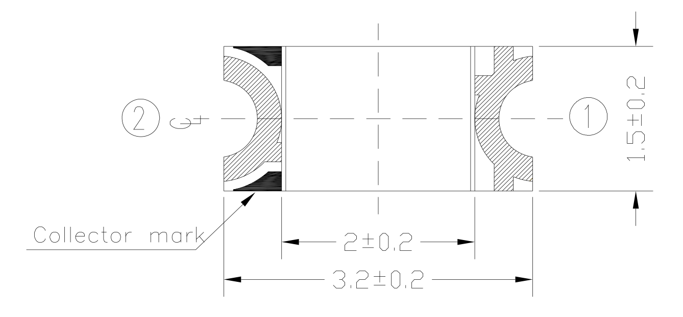
Here is the final soldered PCB:
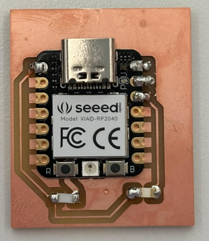
Now, it's time for testing. First, I installed the Arduino IDE on my laptop since I needed it to program the Xiao. Then, I added the RP2040 boards by going to the settings in the Arduino IDE and adding a specific URL (https://github.com/earlephilhower/arduino-pico/releases/download/global/package_rp2040_index.json) in the Additional Boards Manager URLs field. After that, I opened the Boards Manager and searched for “RP2040.” I installed the “Raspberry Pi Pico/RP2040” package by Earle Philhower, which also supports the Xiao RP2040. With the boards installed, I connected my Xiao RP2040 via USB, went to Tools > Board, and selected Seeed XIAO RP2040 from the list. I also selected the correct port (showing up as a new USB device) to make sure it was connected properly. To first test the connection, I used Arduino's blink example code, and it worked!
Then it was time to code! With help from ChatGPT, I wrote this code to see whether the phototransistor could distinguish between light and darkness:
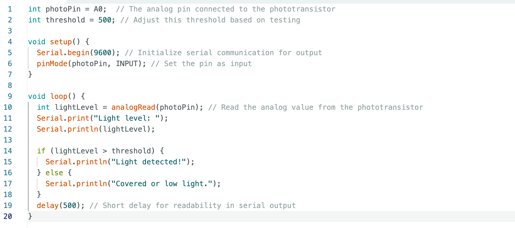
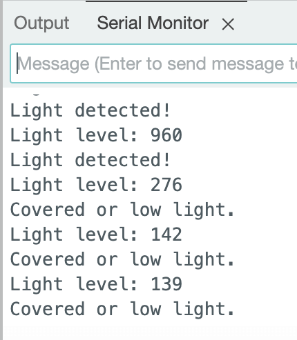
It's very simple code, I set an analog pin for reading the phototransistor, set a threshold value to distinguish light from dark, and printed the results to the Serial Monitor. It actually worked! I could see the light level readings changing based on whether the phototransistor was covered or exposed, which confirmed that the circuit and code were good to go.
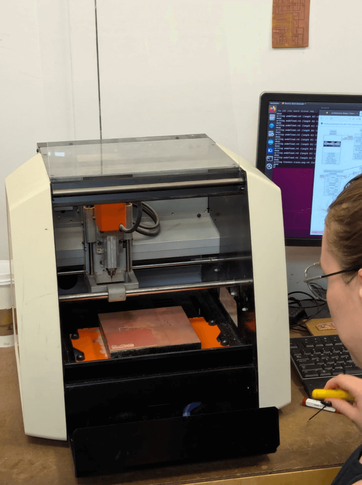
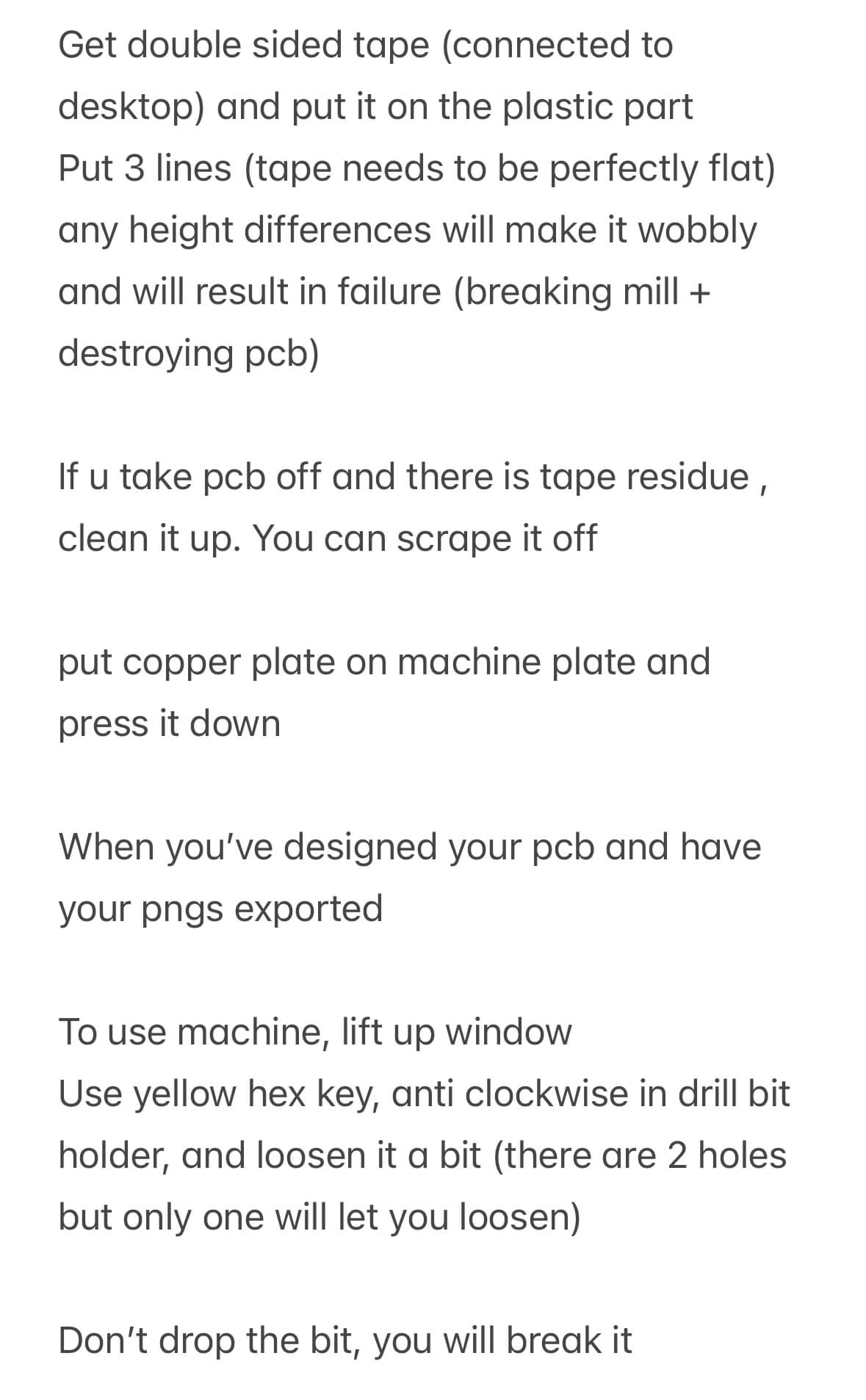
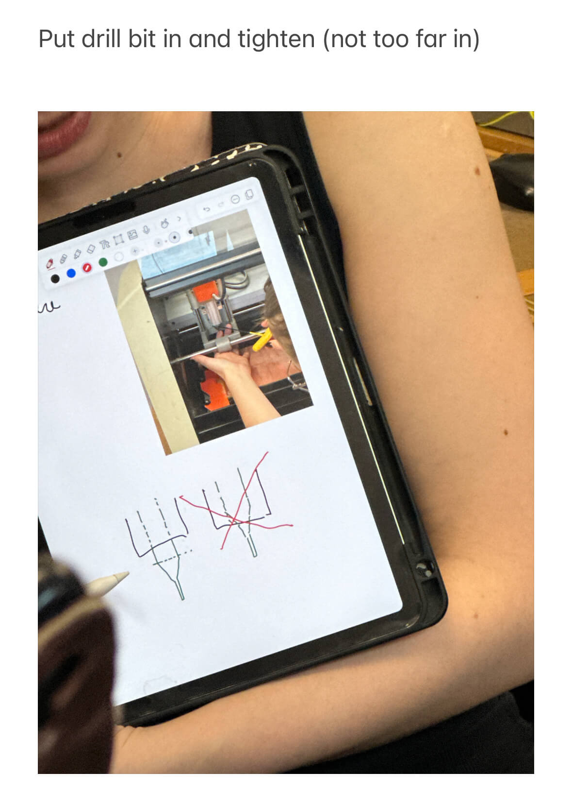
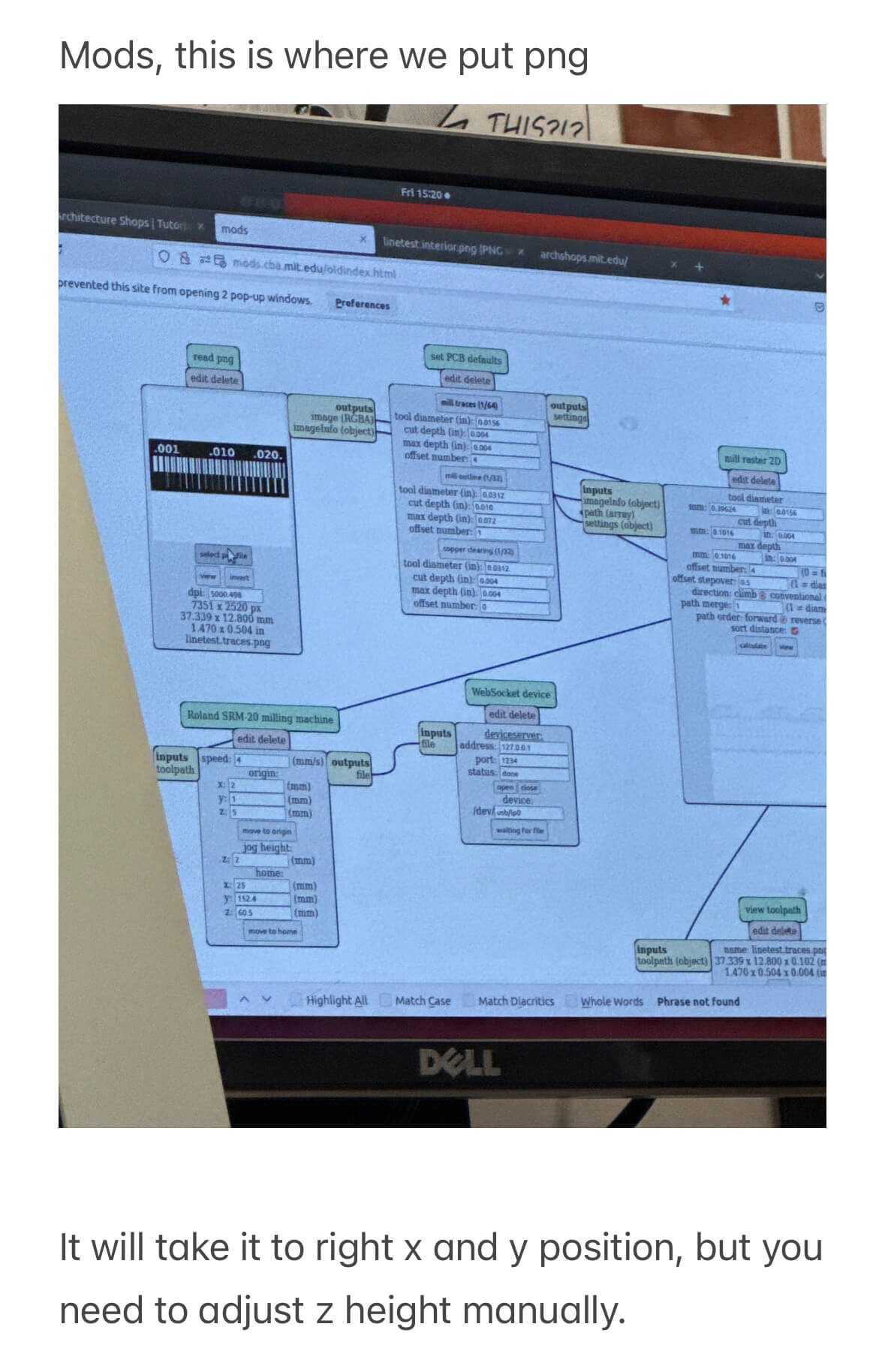
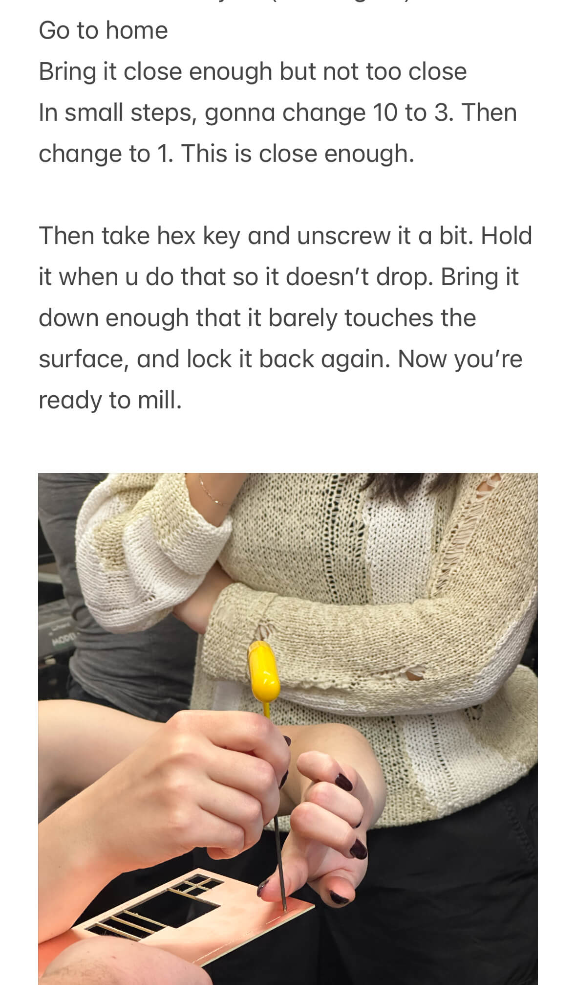
Diana kicked off our training session with a walkthrough of the milling machine in the Archshops. She started by showing how to secure the copper board onto the milling bed with double-sided tape. Next, she explained the bit calibration, pointing out that the 1/64-inch bit is best for milling fine traces and the 1/32-inch bit for cutting edges. We also learned how to import Gerber PNG files into the software and adjust settings like feed rate and spindle speed to avoid damaging the copper.
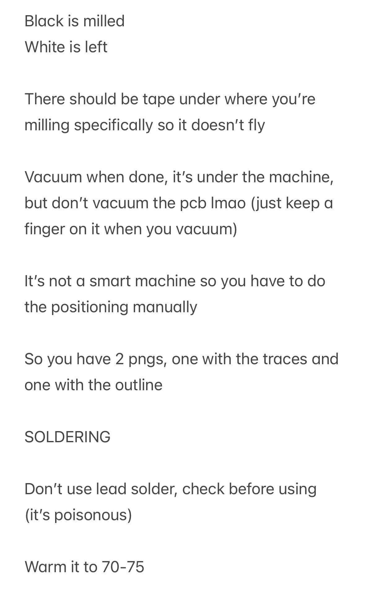
Once the board was milled, Diana had us inspect it closely, using a multimeter to check continuity along the traces and make sure no shorts were hiding between them. She then showed us how to clean the board with soap and water to get rid of any copper bits and prevent oxidation. Moving on to PCB design rules, Diana explained the importance of keeping trace widths above 0.3 mm for solid connections and a 0.2 mm clearance to avoid accidental shorts. For vias, she suggested a 0.6 mm drill size to make soldering easier. She also emphasized using wide ground planes to help reduce electrical noise, especially for components like the ESP32 that are more sensitive to interference.
These are the notes I took:
