Process ✏️
WHAT A JOURNEY! Wow. First, I am so grateful for Leo, Jeff, and the HTMAA Harvard section. I struggled to wrap my head around all of the electronics, but this team was so supportive and helpful.
I went back and forth between what microcontroller to use. ESP32-C3? ESP32-S3? Sense? RP2040? Andddd also what sensor to use.
BNO08X? BNO055? GY 521 mpu 6050? For my electronics production, I am working to create electronics that support a heart rate
sensor and accelerometer. I want the user to be able to view the data on their iPhone or iPad.
I was comparing ESP32-C3 and ESP32-S3.
I determined the ESP32-S3 is the better choice for more computational power for processing the data from the sensors,
or if you think you might expand the project's capabilities in the future to include more complex features. The dual-core
processor and additional features will provide more flexibility for handling multiple tasks and more intensive data processing
directly on the device.
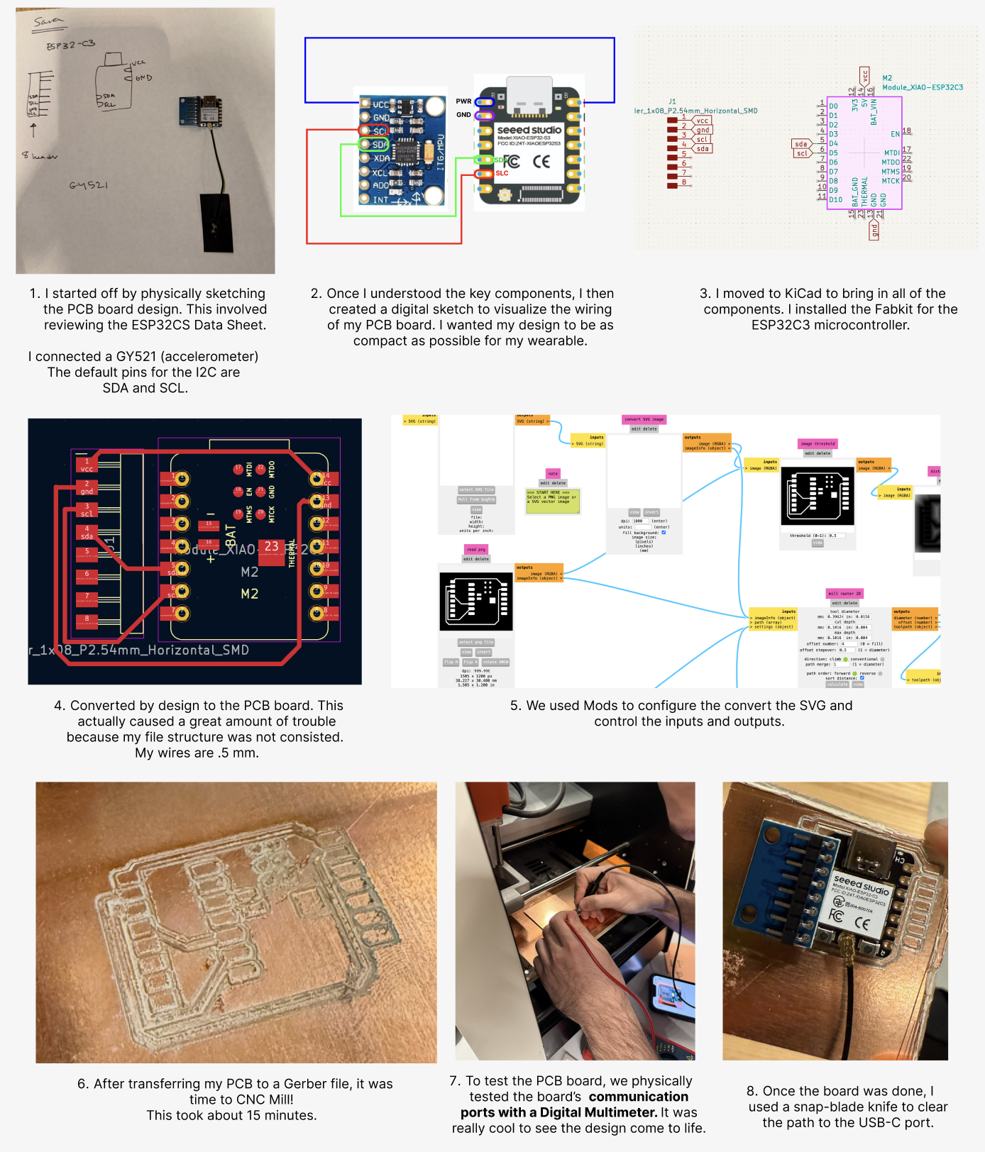
The data sheet was definitely intimidating at first, but once I got to sketching things out… it actually made sense.
The ESP32-S3 is I2C compatible, so I needed to ensure that the sensors I used were supportive of that.
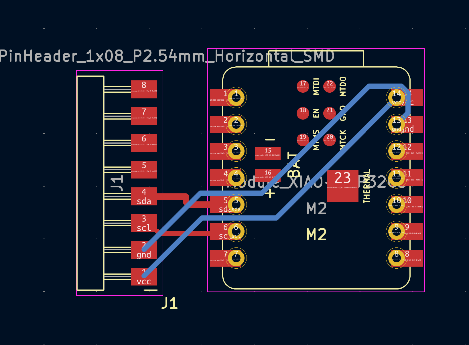
Well, after much debate and research. I decided to use the ESP32-C3 with headers to connect to the GY 521 mpu 6050.
I am amazed how long it took me to do what was such a simple task. I’m starting from scratch to update my schematic and
PCB board design.
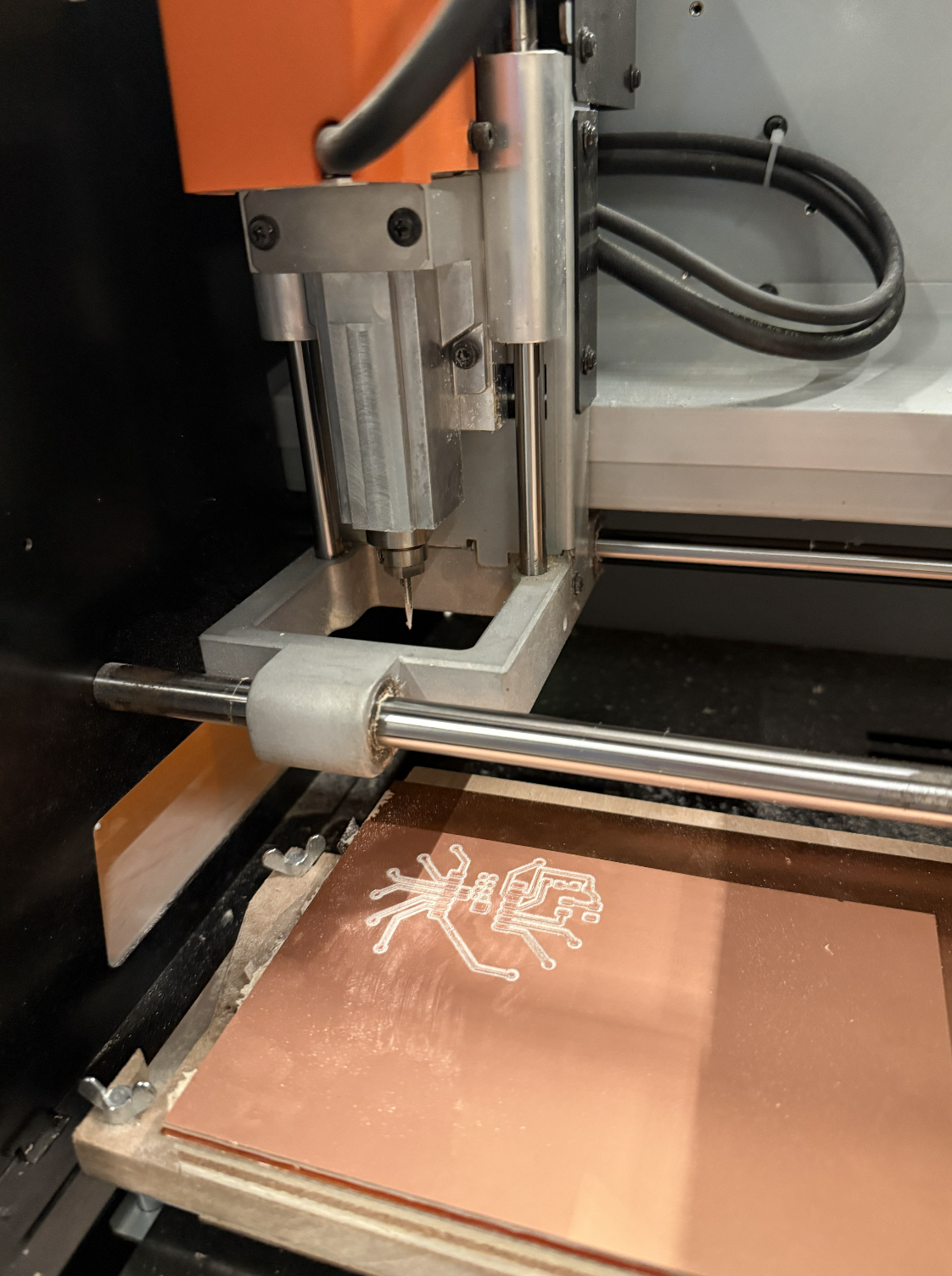
From sketch, Figma, KiCad, CNC Milling, to Soldering!

I sketched things out on paper and layed out all my components. I then migrated things into KiCad. I downloaded the Footprints and the Fab Ki-Cd Master components.
Group Assignment
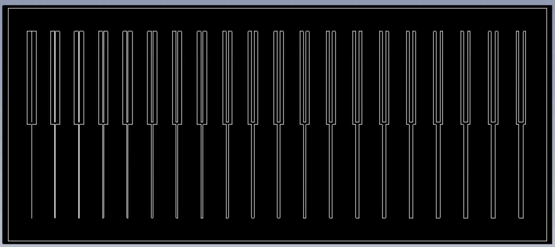
For our group assignment, we worked to characterize the design rules for our in-house PCB production process.
We create a series of rectangles with a Width of the bottom rectangles and top cutouts ranges from 0.001” to 0.020” by 0.001”
increments.


Reflection 🤔
This was the most challenging week for me so far. Knowing that electronics design is not my strong suit, I should have scoped this work differently. Instead, I had a late night in the REEF; but, I learned a lot!
So here’s what I learned:
Deciding on what microcontroller to use
Prototype using WoWiki… rather than designing blindly yikes
Learning KiCad in a week is not an easy task
Go to office hours EARLY in the week! Even if it’s just to run ideas by our wonderful TFs, I think having clarity going into the weekend will be huge.
Moving into next week, I want to continue to flesh out my wearable idea. I know that the Midterm review is approaching on November 13th, so I want to work backwards to set myself up for success.