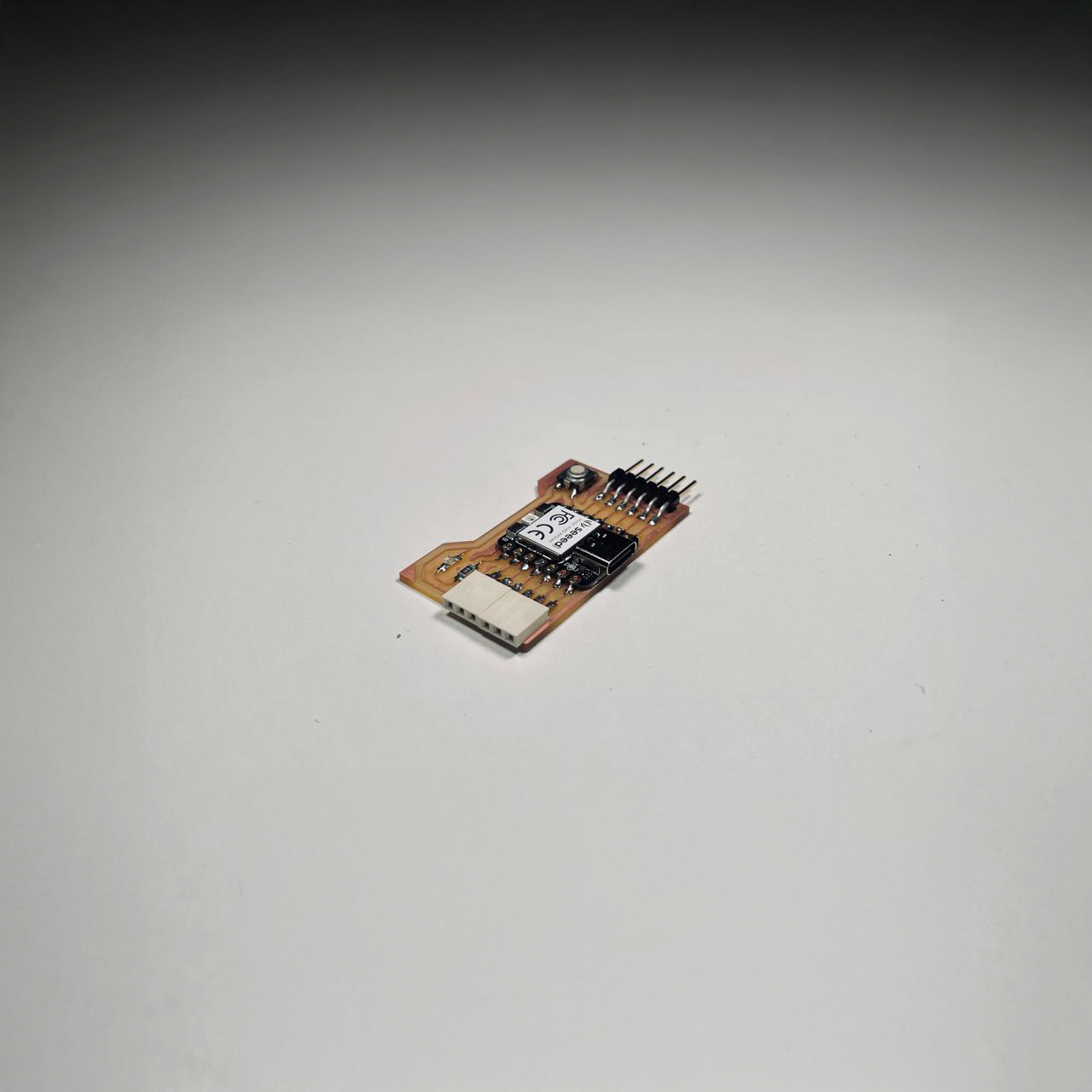
GROUP ASSIGNMENT

With the Architecture Section, we went over the process of milling and soldering a PCB design, which is covered in detail in https://archshops.mit.edu/tutorials.php . Thanks to Diana and Jennifer for showing us the way!

First, we followed the steps for milling a PCB using the two Modela machines in the Architecture Shop. The process involved bringing the design files from Eagle or KiCad, setting up the traces in Mods, and calibrating the machine before cutting. After securing the material, we milled the traces, carefully adjusting for depth and alignment.

Before starting, we gathered our components and placed them on double-sided tape stuck to a small cardboard piece for organization. We made sure the soldering extractor was properly set up to vent fumes. With the solder and iron ready, we allowed the iron to heat up to the correct temperature, getting everything in place for our first joint.

Jenn demonstrated the technique by soldering a small LED onto a sample board. She heated the pad and lead, applying just enough solder for a clean joint. We then placed additional components ourselves and practiced soldering, ensuring each connection was secure while keeping the board intact.


INDIVIDUAL ASSIGNMENT
PCB MILLING
Step 00:
Update PCB Design.
After hearing the lecture on Electronics Production and cross-verifying my PBC design with Quentin, I had to do some adjustments, including dropping some unnecesary capasitors and changing header types.


Step 01:
1/64" Mill Pass.
For the first milling pass, I used a 1/64" end mill to cut the surface traces. I carefully set the material flat on the bed using double-sided tape and calibrated the Z height to cut 0.004" into the copper layer. This ensured the fine connections were clean and precise./p>


Step 02:
1/32" Mill Pass.
In the second pass, I installed a 1/32" end mill to cut out the board outline. I adjusted the toolpath to cut deeper through the substrate, fully separating the board. After milling, I cleaned the bed and removed debris.


PCB SOLDERING

Cleaning up the board.
This is necessarry to ensure proper flow of the solder in the board and facilitate the creation of proper connections

Setup.
Before Soldering, I looked for all the components I neded and placing them on a cardboard with double-sided tape. Then, I set up a magnifying glass, a fume extractor, some solder, and the soldering iron

Step 00:
Starting State
With everything in order and the pcb clean and ready to go, I heated up the soldering iron to 370 degree celcius for my lead-based solder.

Step 01:
Point Connections
Following our TA's recommendations, I started by meltng drop of solder into 1 connection per component.

Step 02:
Component Placement
Next, I used the soldering iron in one hand to heat ad liquify those points, while I placed each component in place with the tweezers.

Step 03:
Complete Soldering
With each component in place, I proceeded to add solder to all of their other connections, ensuring solder linked the piece and the board's connection point.


Step 04:
Review Connections
Finally, using the microscopes in the architecture shop, I double-checked that all connections


PCB PROGRAMMING
Testing D7 LED

Testing D0-D10
with external LED

Testing D6 & D7
Switch Controlling D7 LED
