← Back to Main Site
Week 6: Electronics Production
Gratitude this week to: Gert, Adin, Carlos, Stasya, ChatGPT, and (again) my tattoo artist Anupriya (see Ironbuzz Mumbai)
Group Assignment
Characterize the design rules for your in-house PCB production process
This week, we explored the workflow of using a Roland milling machine to cut and fabricate our own PCBs. The design rules included trace width and spacing (some of which Quentin went over last week).
For Gert's training, we used a test design that had been preloaded onto the computer. Here's the workflow documented (both for me and anyone else new to this)
Prep
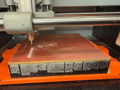
- 2 options to mill the PCBs; we’re using the Roland SRM-20. documentation is on the website
- roland has a mods page accessible on the computer in the lab. like the vinyl cutter, we put in a b&w image, calculate the toolpath, & send it to the device
- scrap copper boards are available in the box or big cabinet. there’s a measure tool in KiCad — you can (and should) measure before choosing what size board
- context: PCB boards are a thin layer of copper over some plastic. when we excavate, we’re just removing some copper so that it acts like a wire. that’s more stable than wires on a breadboard.
Process
- we cut the traces and then the outline (because doing the reverse messes with the stability - it might shake when the traces are being cut)
- for milling & tracing, we use a drill bit called an endmill to excavate the copper. we have 2 kinds — 1/64th & 1/32. we use the latter for cutting the outlines. excavating the whole PCB out of the main sheet. we use the former for the traces, because you can get more detail. (these are stored in the small shelf behind the computer)
- the piece of copper already on the milling machine is called the spoil board. this can influence the success of our cut if it’s not flat
- tape your piece of copper to the spoil board. you can go completely overboard here but you should make sure the tape is flat. at the very least, you should do perpendicular pieces, at least 3 (cc Gert's superstitions). Don't overlap any tape as this will ruin the flatness/texture.
- Best practice here: use the flat yellow icing smoothener looking thing to stabilize and stick the copper piece to the spoil board
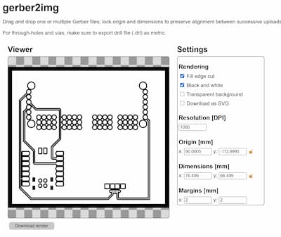
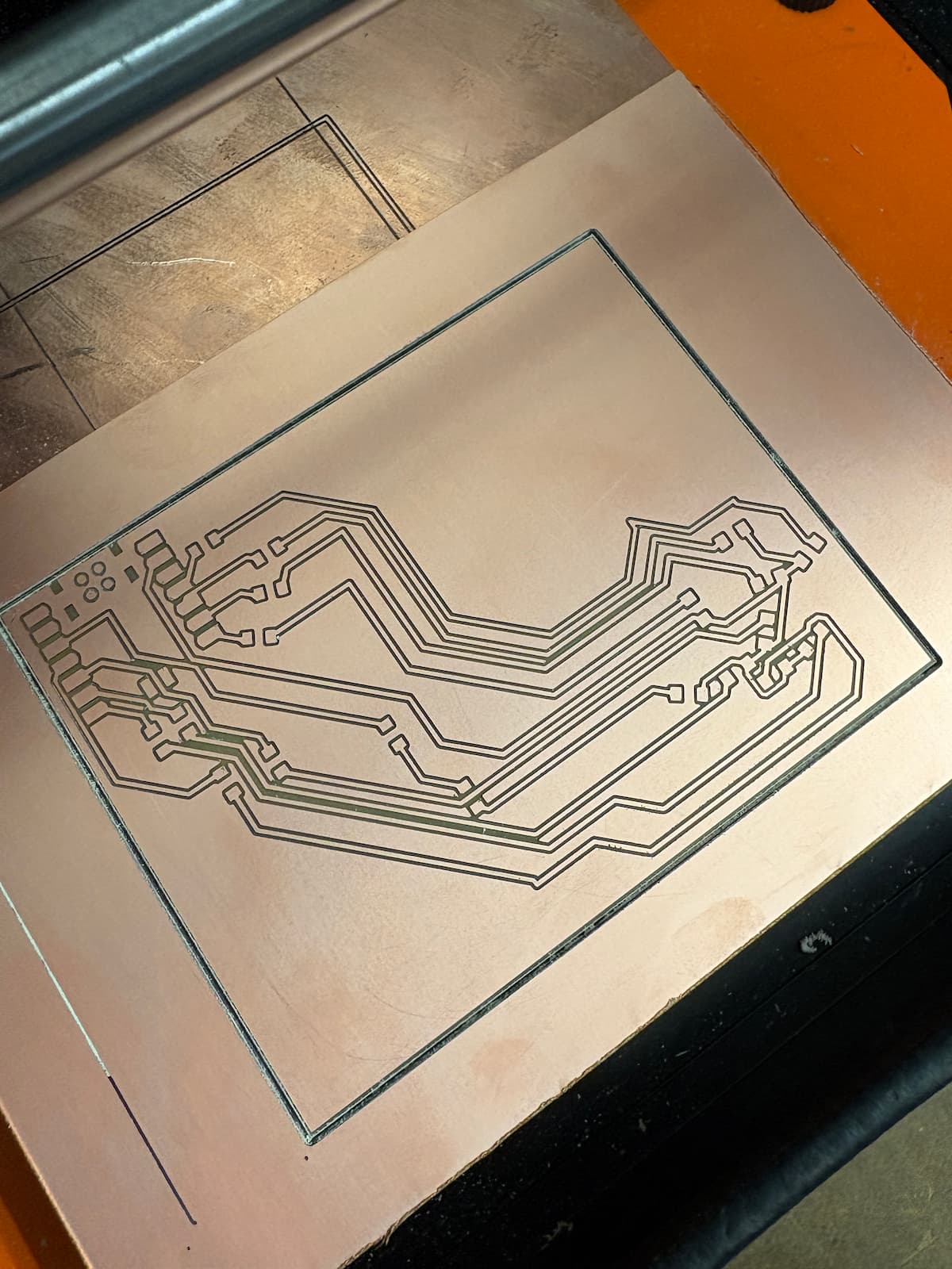
- have 2 png files ready: one for the traces and one for the outline. 2 separate. use Quentin’s gerber2image tool
- install the endmill - use your thumb/finger to push it in as far as possible (more than it should be), then use yellow allen key to twist it in
- make sure the green light on top isn't flashing
- select png file —> select “mill traces” —> press calculate under mill raster 2D
- set your origin correctly — it’s the bottom left. websocket > status > open; calculate; send file to device
- vacuum using the festool on the side when traces are done
- next, switch to the 1/32 endmill for the outline, and upload the new png. select image > trace/outline > set origin > calculate > open on socket > send file to device > vacuum

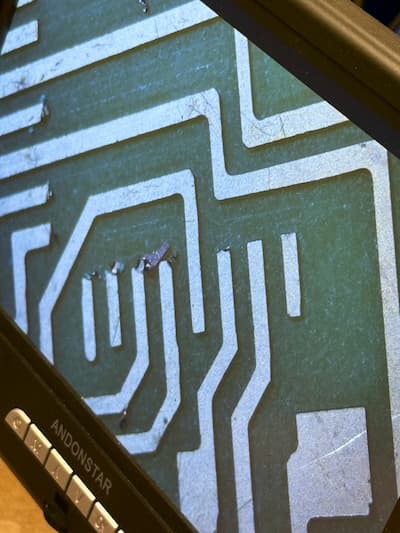
As you can see, the magnified practice cut is not clean -- so Gert also showed us how to clean it otherwise it would short. I've also documented some of Gert's best practices down here.
Also, fun fact: throughout my notes I've spelt "endmill" as "inmill". What a trip to be here.
Best practices
- Optional, but put your PCB on a breadboard before to test the components, whether they work together, etc. before committing to soldering / production
- be very delicate with the endmill, otherwise it can shatter
- "broken endmills look like cold broken chocolate" - Gert
- similar to laser cutting, we need copper that’s as flat as possible, no warps. zero bends. thats why it’s often better to have a small PCB - larger copper pieces are more prone to bending
- make sure the spoil board is flat
- make sure the drawer below the spoil board is closed and glass door is closed. green light on top should not be flashing
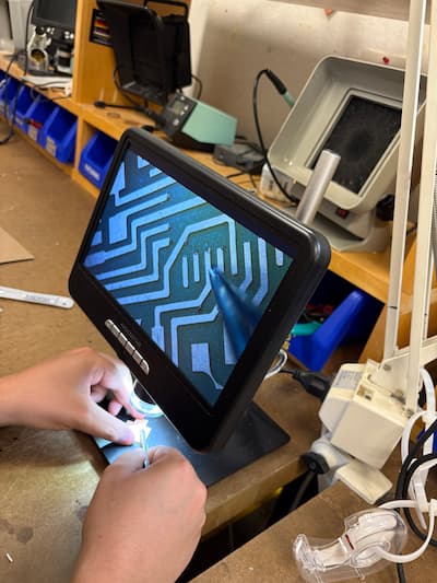
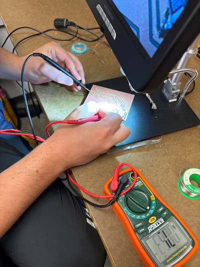
- check your board under the microscope, test for any excess material, loose connection. use a multimeter to be sure.
Submit a PCB design to a board house
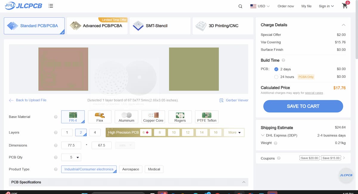
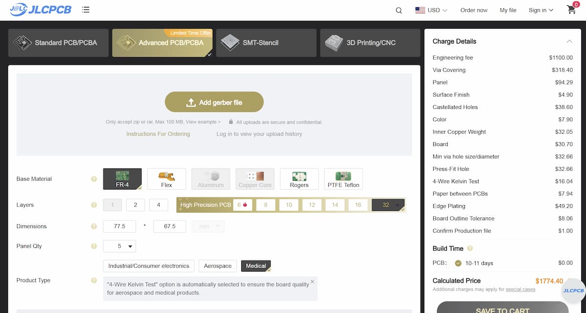
This week, Stasya uploaded her PCB design to JLCPCB to produce a professionally manufactured board. The last image is them trying to make this as pricey as possible. This is crazy.
Individual Assignment
What we’re trying to do this week
Make and test an embedded microcontroller system that you designed
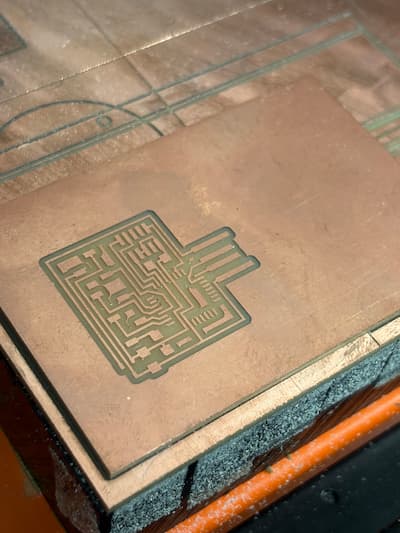
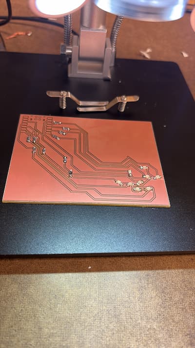
Yet another cool industrial machine I've never used! I originally wanted to print the cat design I made last week, and actually made some progress to that effect:
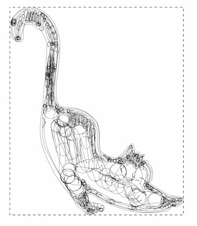
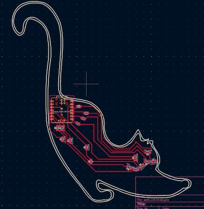
But eventually I realized that as it stands, this cat outline is enormous, and the tail would extend out of the copper boards we're using. I'd want to rearrange the components within its body to be a bit simpler and make the cat smaller to not waste too much copper. So, at least for the first go, I retained the body shape with the traces and made the outline a square.
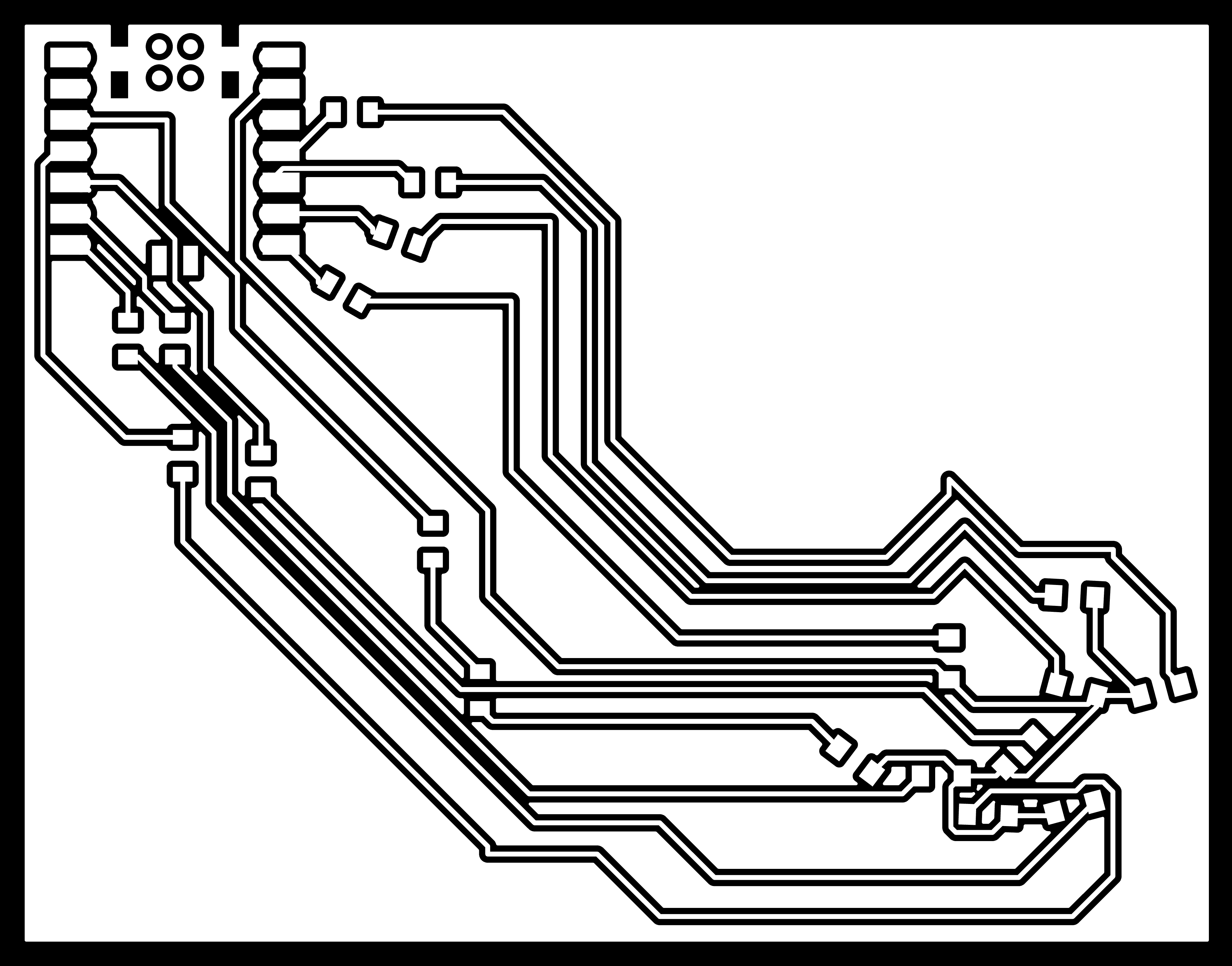
If you're curious though you can download my cat svg below. I've also included my cat traces and another square outline.
Attempt 1
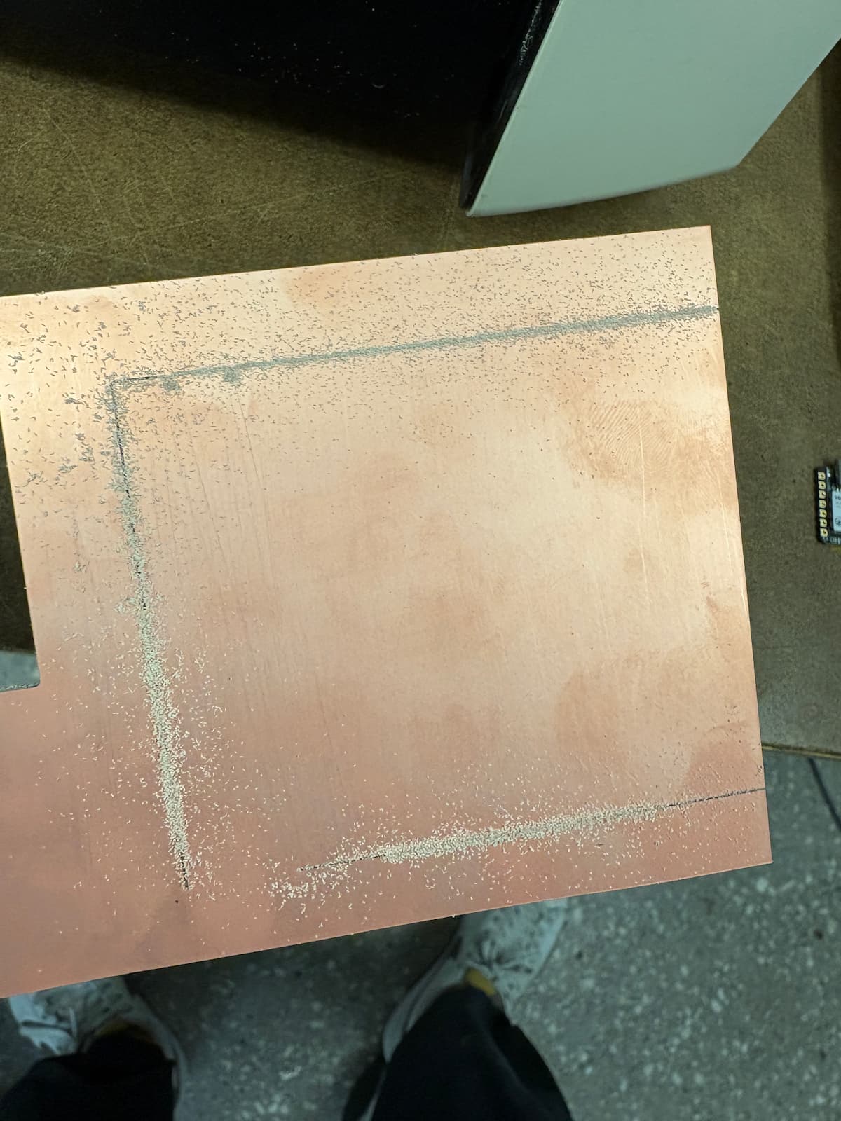
Big thanks to Adin for patiently sitting through this with me (and for knowing this machine like the back of his hand). On my first attempt, I was trying to use a large copper board that had a tiny piece already soldered off the left. I thought this would be okay, but the mistake was I forgot to use measure in Kicad, and so I didn't realize the endmill would fall off the edge. You should never vibe cut.
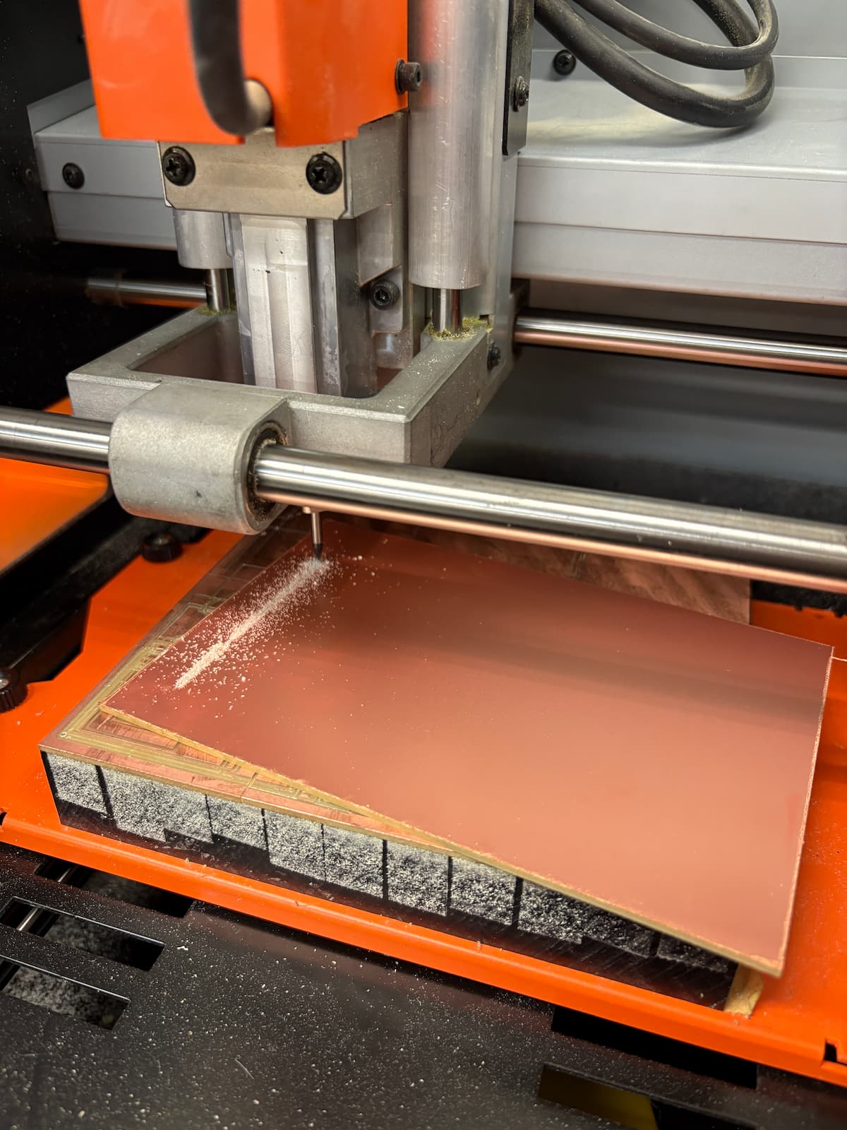
Attempt 2
Second attempt: fresh copper board. Put the tape around the perimeter as we'd discussed. But wasn't bold enough with tape, and didn't use the trusty icing smoothener. So the piece just... moved off on the spoil board. So I went ham on the next try.
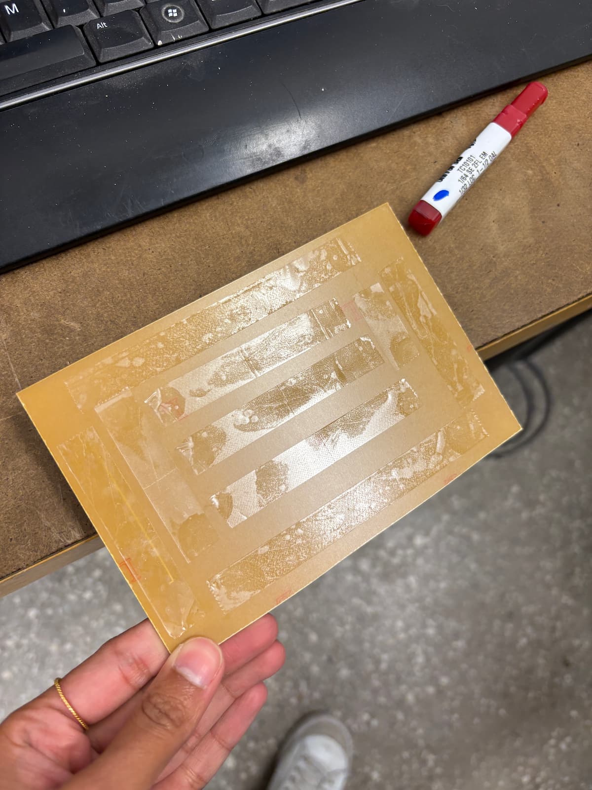
Attempt 3
Third time's the charm?
Soldering
ICYMI from prev weeks: not too good at soldering. So I treated this as a great opportunity to just get reps in.
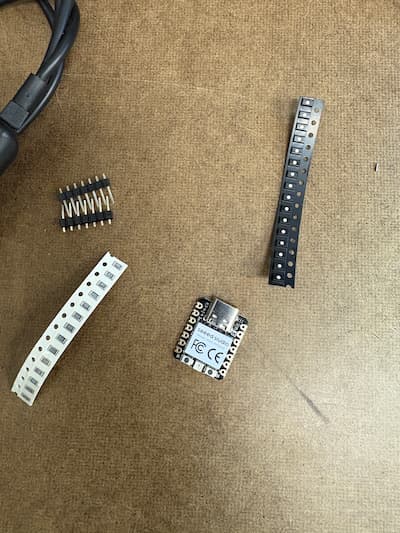
These are the components I was working with, from the inventory. Did the math: from the datasheet on DigiKey I learnt that the LEDs have a forward voltage of 2-2.4V and a max forward current of 25 mA. I wanted around 10-15 mA. Also, learnt that you get 3.3V from the XIAO's onboard regulator. So, R = (V(supply) - Vf)/I = 3.3v-2.2v/0.015A = 73ohm. Don't have this, so used 100:
- XIAO RP2040
- LED Green Clear 1206 SMD - 9 nos.
- 8 100 Ohm Resistors
- 1 0 ohm resistor
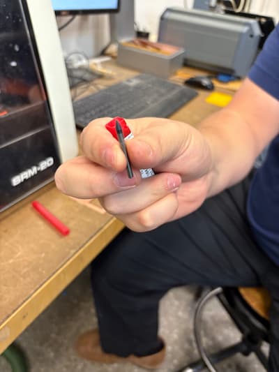
Then moved on to soldering, in the order of resistors (easiest) > LEDs (had to learn to identify cathode vs. anode, and learnt cathode to GND, anode to resistors > XIAO (hardest to solder).
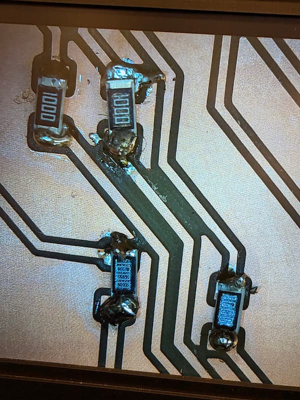
We tested it using a multimeter, and it was beep city. Big thank you to Gert though for helping me clean up + attempt to fix shorts late into the night.
I ran out of time to fix that this week, but here's what I'd do differently next time:
- practice soldering first on a practice board
- instead of feeding the wire, try putting a bit of solder on the tip of the iron pen and letting it melt onto the pad
- I read somewhere that you don't actually need a ball of solder - it just needs to be enough to wet the pad. I don't think this is true -- none of my components stuck this way. So will probably watch someone do it who knows better than me.