week 5:electronics design
Installing Kicad and libraries
This week’s assignment focused on getting started with PCB design using KiCad, including installing the software and setting up the necessary libraries. The initial step involved familiarizing myself with the interface, understanding how components are organized, and ensuring that all standard and custom libraries were correctly installed. This setup was essential for creating accurate and functional designs in the following tasks.
Group training
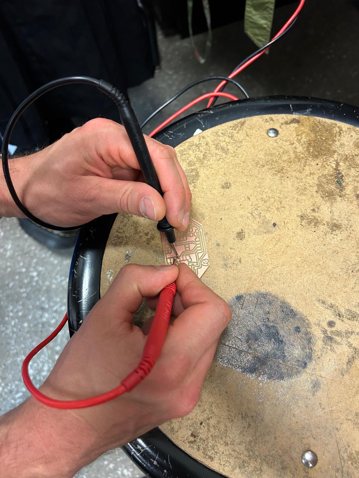
This week, Gert provided us with the essential knowledge to use a multimeter, a fundamental tool for testing and troubleshooting electronic circuits. Learning to use the multimeter allowed us to check if our soldering was done correctly and to quickly identify errors such as open circuits, short circuits, or incorrect connections. By measuring voltage, current, and resistance, we gained the ability to verify that each component and connection on our boards functioned as intended before moving on to more complex testing.
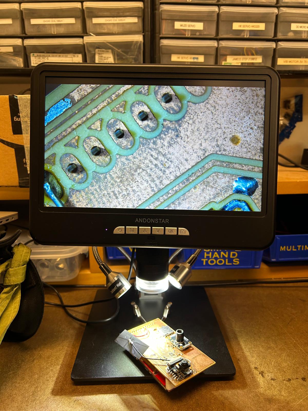
We were also introduced to the microscope as a tool to assist with soldering. It allowed us to closely examine small components and connections that are difficult to see with the naked eye.
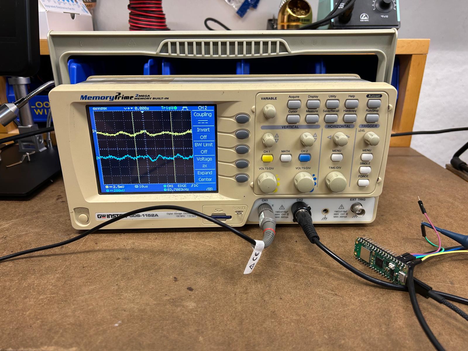
In addition to the multimeter, we were introduced to the oscilloscope, another powerful diagnostic tool. An oscilloscope allows us to visualize electrical signals over time, displaying waveforms that show how voltage changes dynamically within a circuit. This makes it possible to analyze signal behavior, detect noise or fluctuations, and troubleshoot timing-related issues that a multimeter cannot reveal. Understanding how to use these tools was crucial in preparing us for the next stage: electronics production.

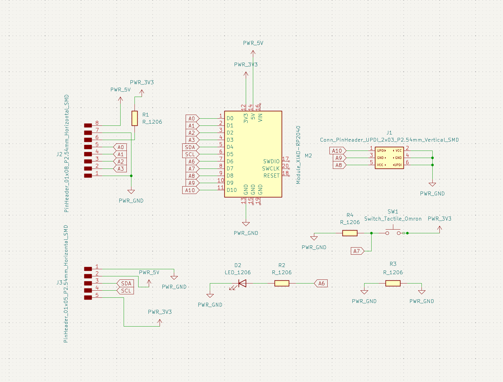
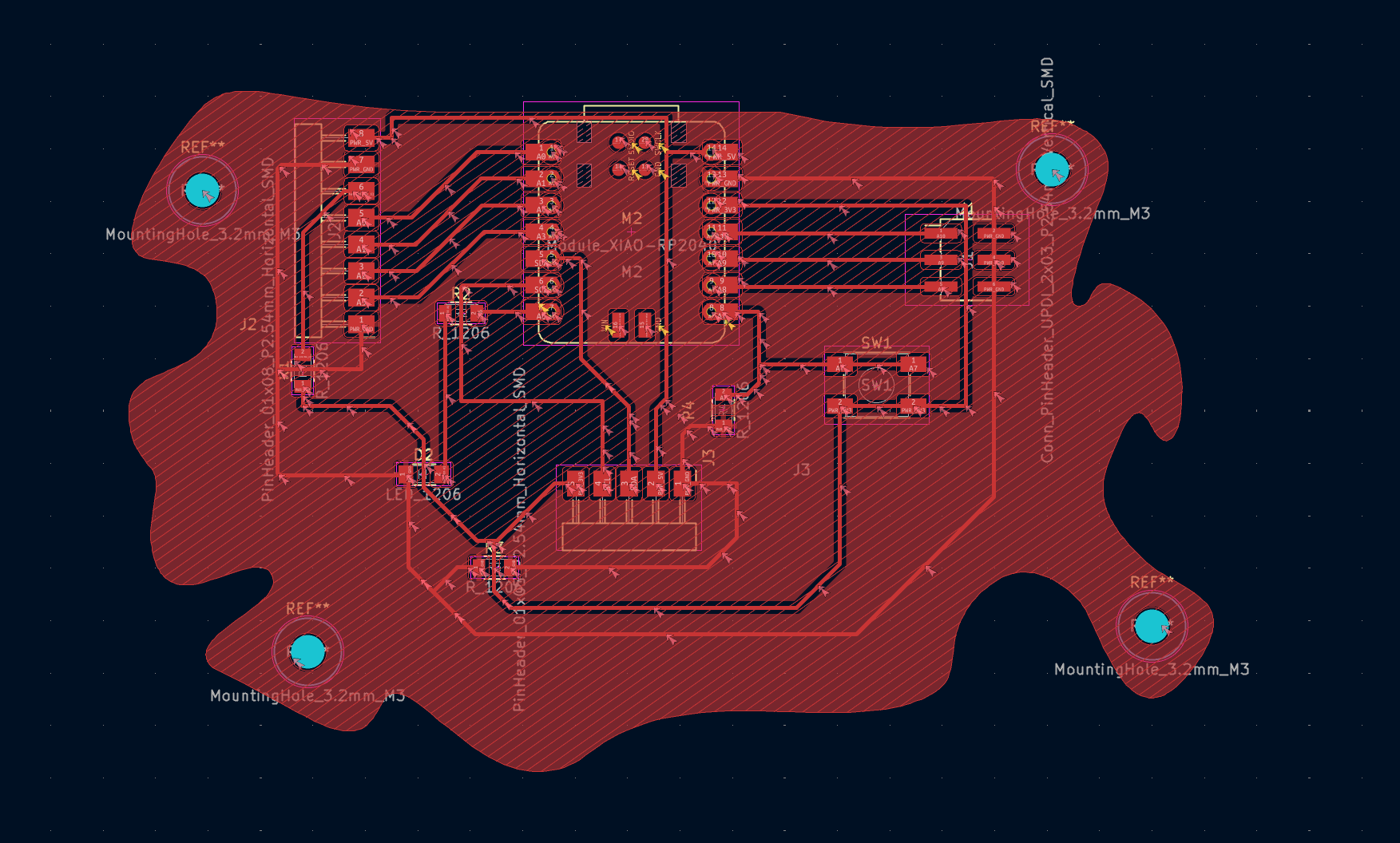
Board design
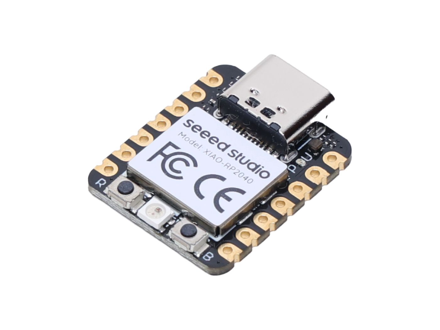
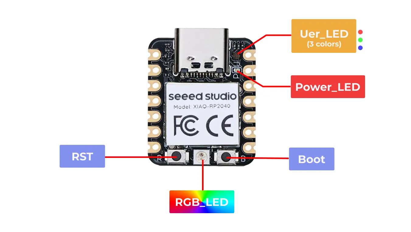
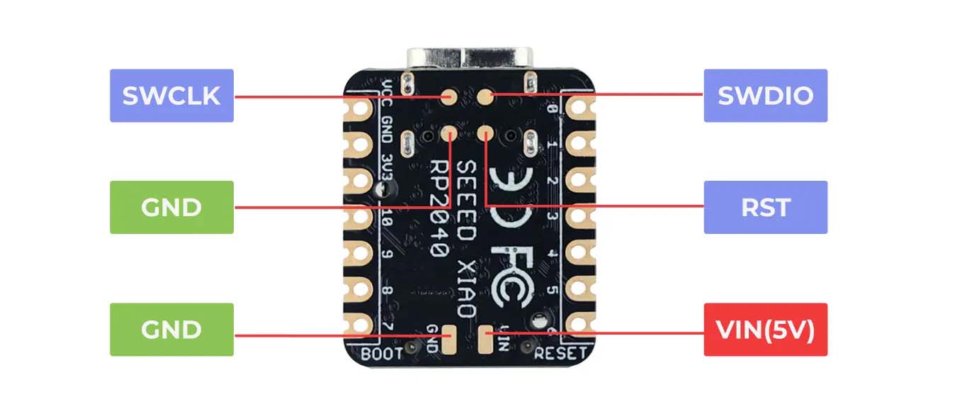
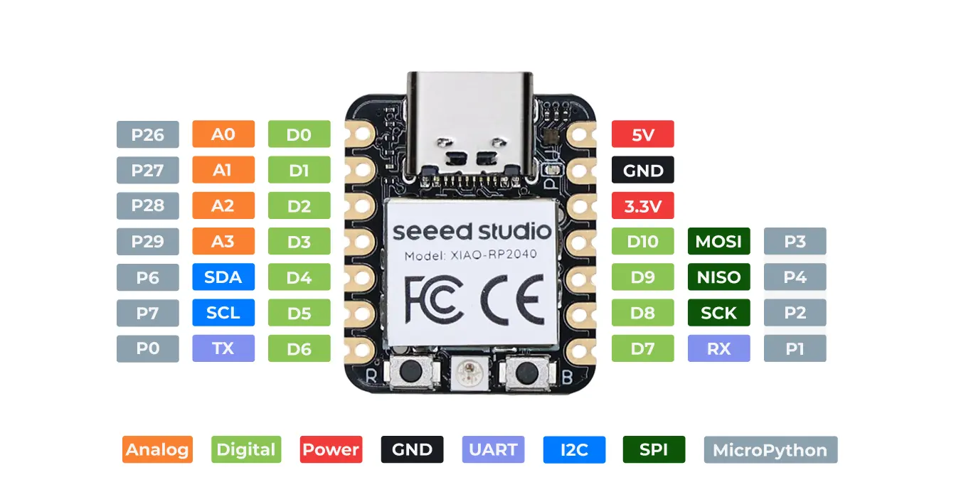
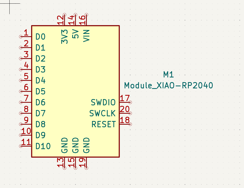
Before I started designing my PCB board, I realized it was important to gain a deeper understanding of the components I would be using. One key component was the Seeed XIAO RP2040 microcontroller, which we had already encountered during week three’s embedded programming exercises. Since this microcontroller would serve as the central element of my board, it was essential to understand its specifications, capabilities, and limitations in detail.
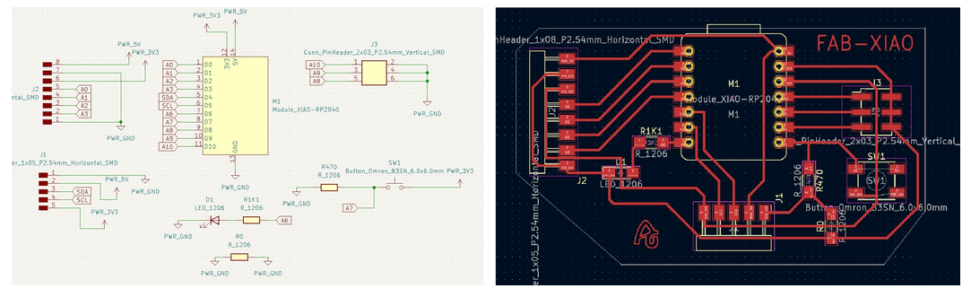
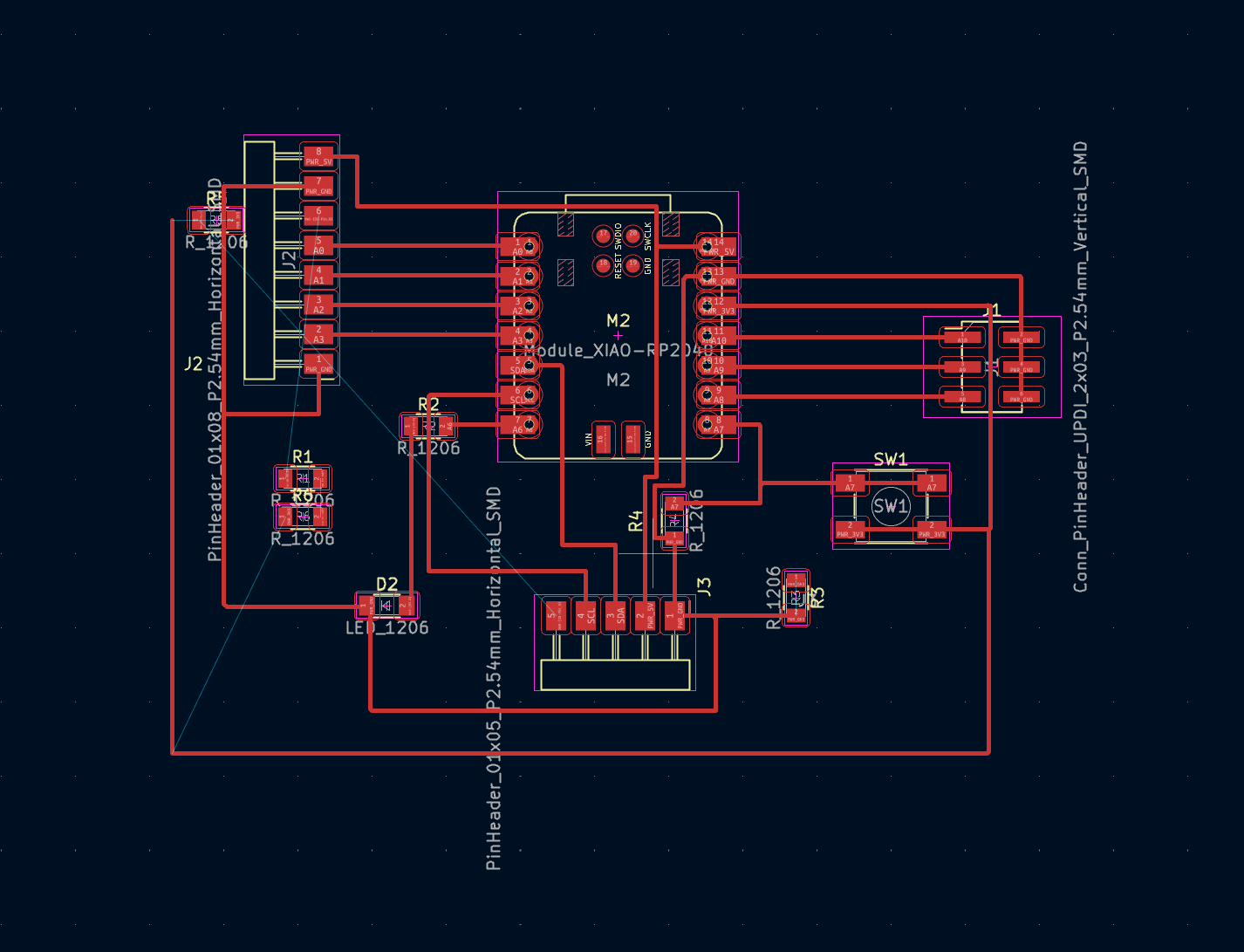
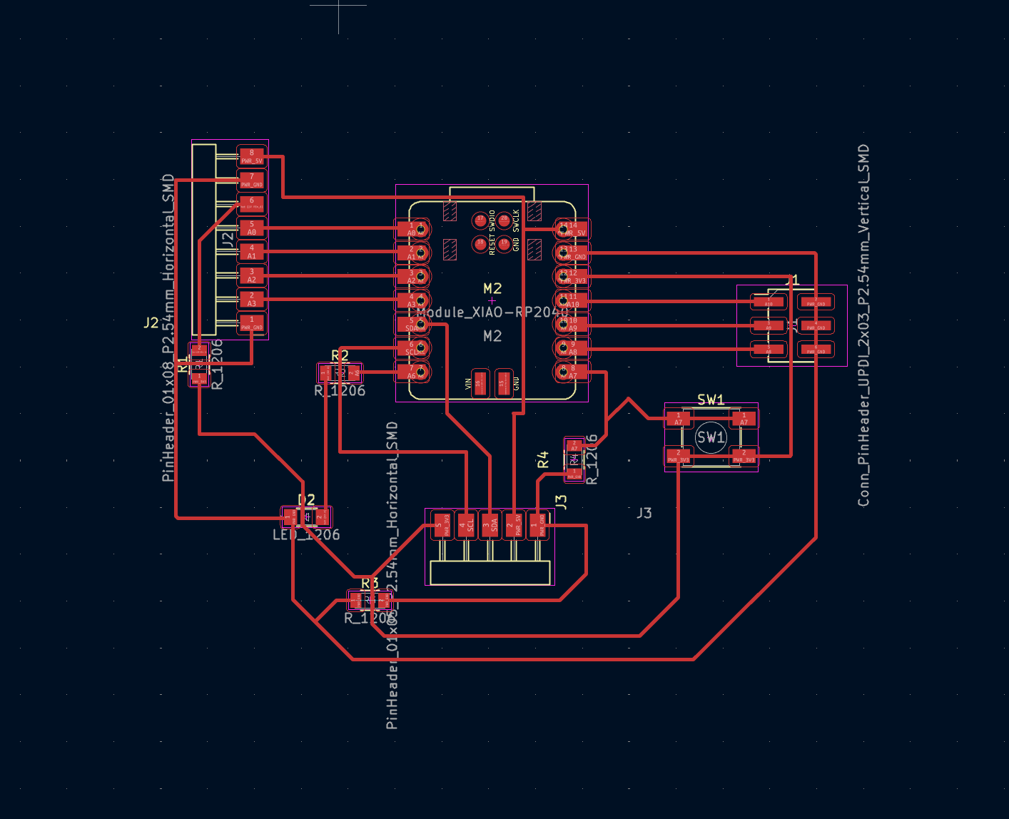
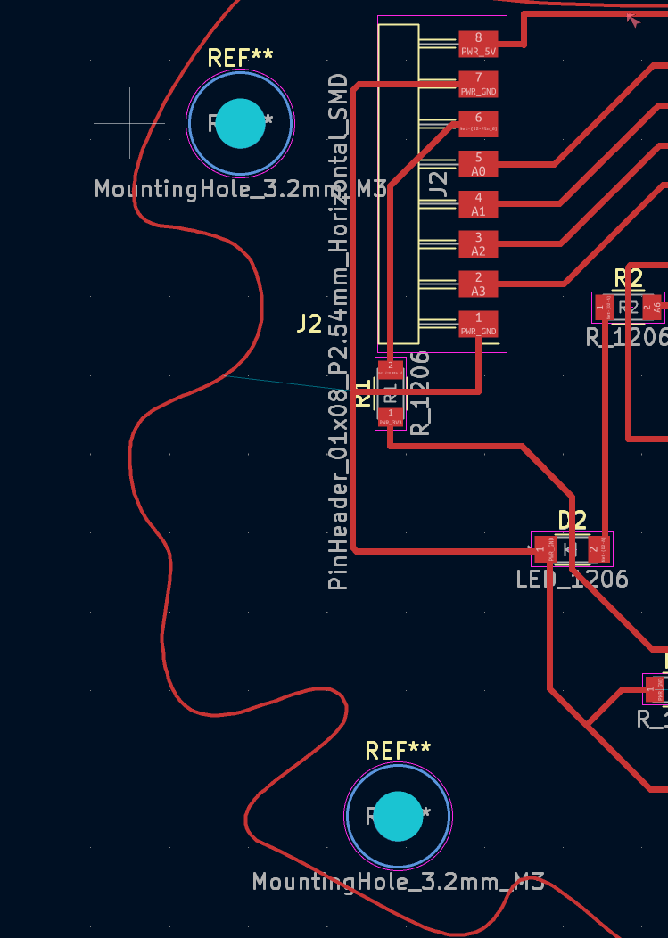
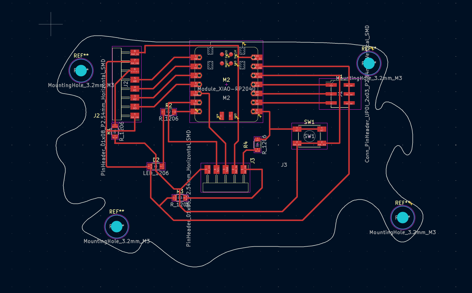
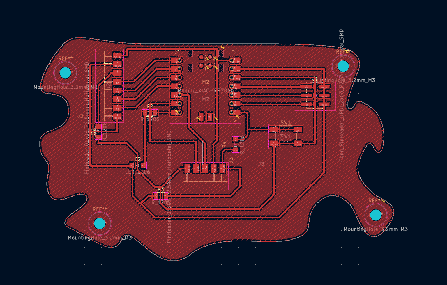
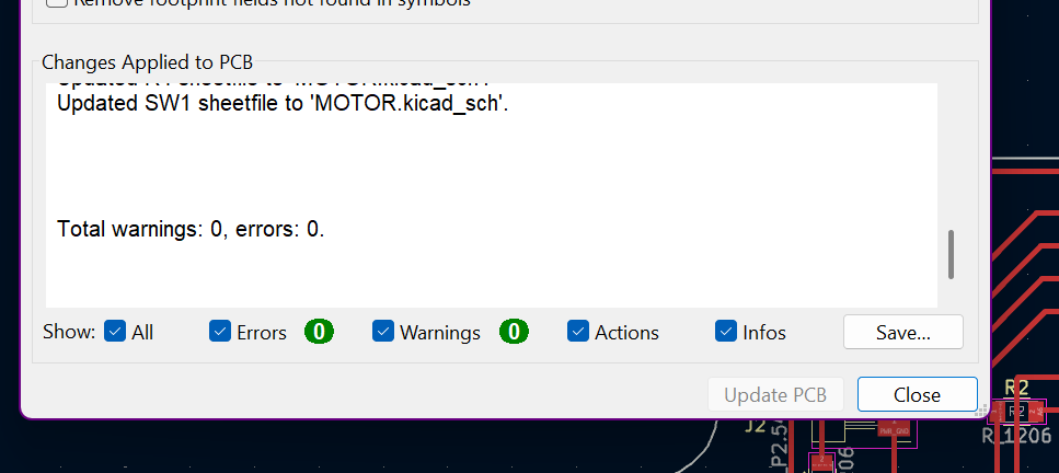
At this point, after understanding the basic connections required for the RP2040 microcontroller and having a reference board design, I focused on familiarizing myself with the KiCad software. I explored the schematic interface to understand how components are placed, how electrical connections are defined, and how nets are organized.
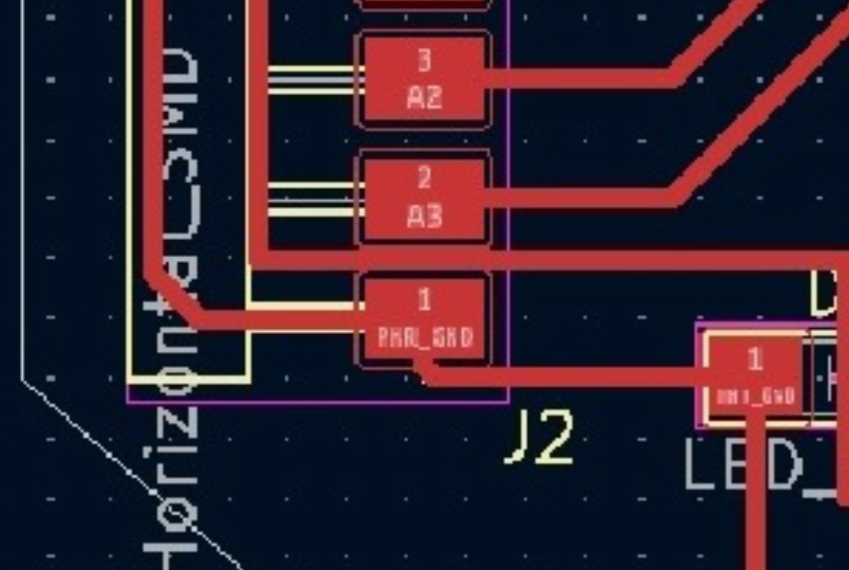
I then examined the board design interface to see how the schematic information translates into a PCB layout, including component footprints, trace routing, and board constraints. Moving between the schematic and layout views made it clear how changes in one environment affect the other. This process was less about finalizing a design and more about understanding the workflow, tools, and relationships within the software.
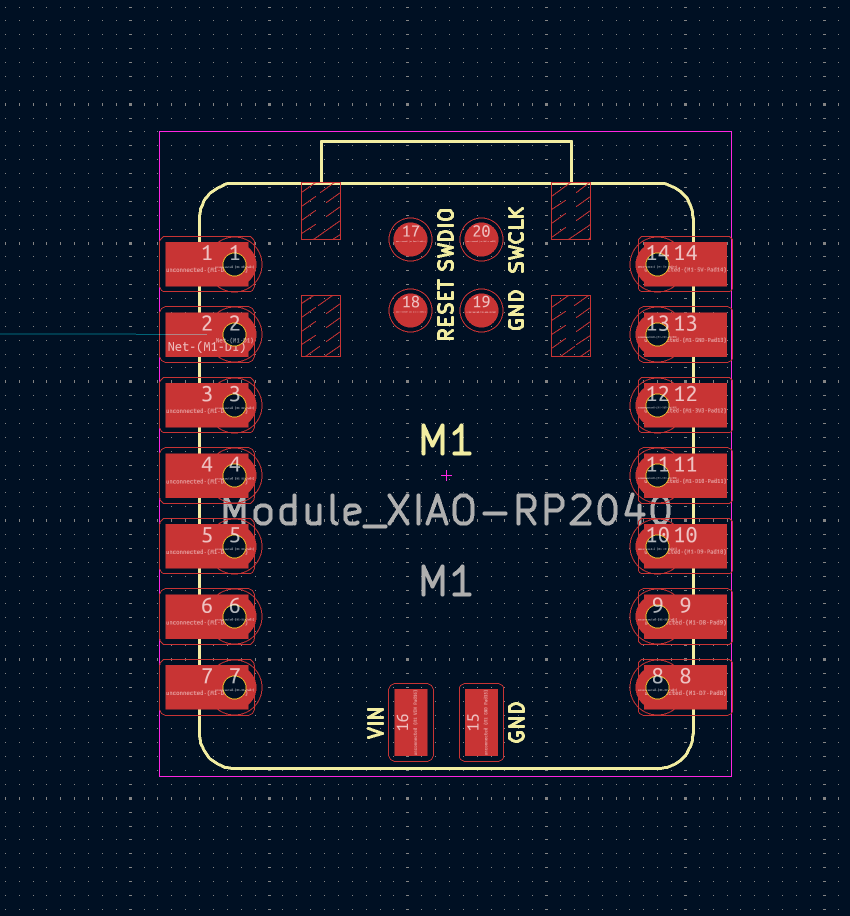
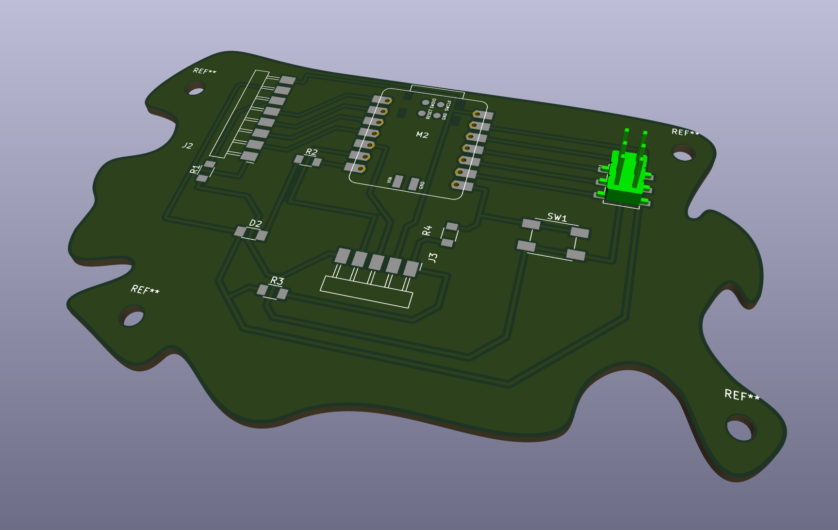
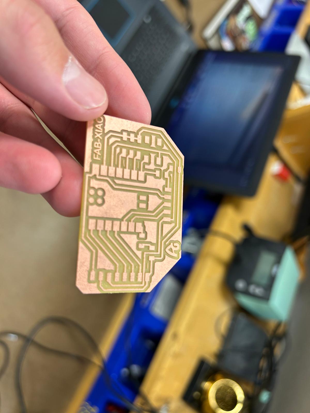
After becoming familiar with the KiCad workflow, I decided to base my design on the Fab XIAO board layout. This choice was motivated by the large number of pin header connections available on that board, which offer flexibility for future use. Having many accessible pins makes it easier to connect external components, sensors, and modules without redesigning the board each time.
By examining the Fab XIAO design, I was able to understand how the microcontroller pins are broken out and organized in a clear and practical way. This reference helped clarify how power, ground, and signal pins can be arranged to support multiple applications. The goal at this stage was not to customize the board for a specific function, but to create a versatile platform that could be reused and adapted later. Designing around a proven reference also reduced uncertainty and helped reinforce good layout practices.