Assignment Overview
Assignment Requirements:
• Use an EDA tool to design an embedded microcontroller system
• Use parts from the Fab Lab Inventory
• Check design rules for fabrication
• Design for manufacturability in the Fab Lab
This week's work covers:
• Introduction to PCB design workflow and methodology
• KiCAD schematic capture and symbol library management
• PCB layout design and footprint assignment
• Design rule checking and 3D visualization
• USB interface design and connector integration
• Gerber file generation for manufacturing
Learning Objectives
• Understand the complete PCB design workflow from schematic to layout
• Master KiCAD EDA tools for electronics design and visualization
• Learn to select components from the Fab Lab inventory for embedded system design
• Learn proper component symbol and footprint selection
• Develop skills in PCB layout and routing techniques
• Implement design rule checking (DRC) for Fab Lab fabrication
• Design embedded microcontroller systems with proper interfacing
• Create manufacturing-ready design files for fabrication
Work Completed
KiCAD Tutorial Project
• Followed KiCAD 7 PCB Layout in 5 steps tutorial by The Design Graveyard• Completed comprehensive KiCAD tutorial to learn PCB design fundamentals
• Created schematic with USB connector and supporting components
• Designed PCB layout with proper routing and component placement
• Generated 3D visualization of the final board design
Schematic Design
• Created circuit schematic using KiCAD Schematic Editor• Added USB Type-B connector symbol from KiCAD library
• Connected USB power and data lines with proper net labeling
• Performed electrical rules check (ERC) to verify design
• Generated netlist for PCB layout import
PCB Layout Design
• Imported netlist into KiCAD PCB Editor• Assigned footprints to all schematic symbols
• Placed components with consideration for signal flow
• Routed traces following best practices for USB signals
• Added ground plane and proper power distribution
• Performed design rule check (DRC) for manufacturing compliance
3D Visualization and Verification
• Generated 3D model of PCB with component placement• Verified mechanical clearances and component heights
• Checked USB connector orientation and accessibility
• Validated overall board dimensions and mounting holes
Tutorial Project: Learning KiCAD Workflow
Project Overview
Completed a USB connector tutorial project following the KiCAD 7 PCB Layout in 5 steps tutorial by The Design Graveyard to learn PCB design fundamentals using KiCAD EDA tool. This prepares for future embedded microcontroller system design using Fab Lab Inventory components.Key Learning Points
KiCAD Design Workflow (Schematic → PCB → Fabrication): 1. Schematic Capture: Select symbols, place components, wire connections, run ERC2. Footprint Assignment: Link symbols to physical footprints with 3D models
3. PCB Layout: Define board outline, place components, route traces, add ground planes
4. Design Rule Check: Verify design meets Fab Lab fabrication rules
5. Manufacturing Output: Generate Gerber files and drill files
USB Differential Pair Routing: • Keep D+ and D- traces length-matched and parallel
• Maintain 90Ω differential impedance
• Use continuous ground plane under USB traces
Fab Lab Design Rules for Fabrication: • Minimum Trace Width: 0.4mm (16 mil)
• Minimum Clearance: 0.4mm (16 mil)
• Minimum Drill Size: 0.8mm
Component Selection for Future Projects: • Use Fab Lab Inventory for standardized components
• Check component availability before finalizing designs
• Common categories: Microcontrollers (ATtiny, ATmega, SAMD, ESP32), connectors, passives, sensors
Images
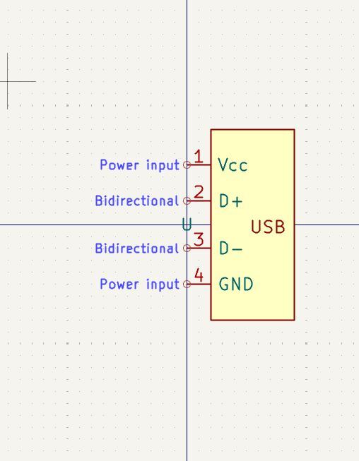
USB Type-B connector symbol selected from KiCAD schematic library
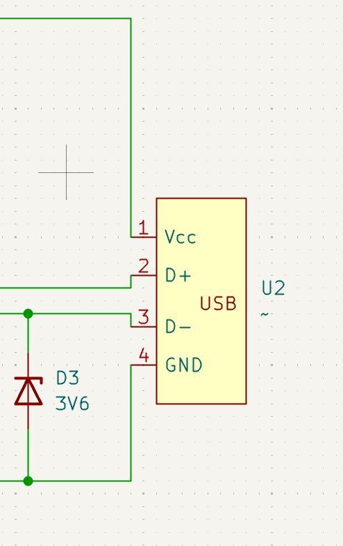
USB connector symbol with power and data lines connected in schematic editor
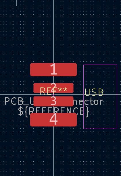
USB connector footprint assigned with physical pad layout and dimensions
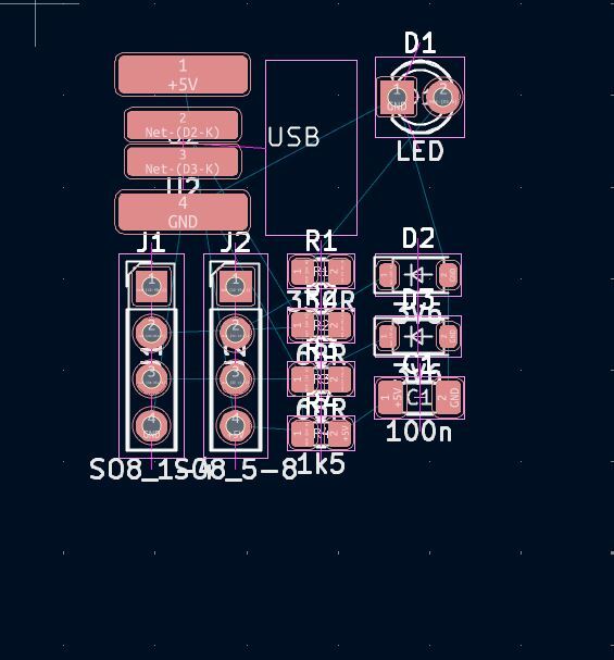
KiCAD PCB editor showing component placement and routing in progress
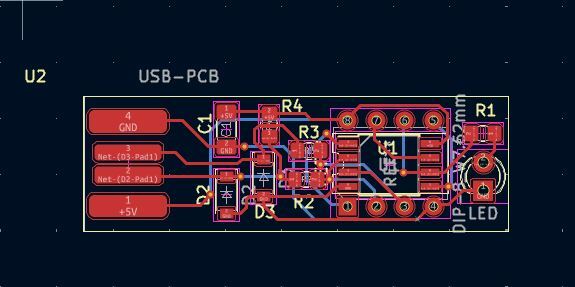
Completed PCB layout with all traces routed and ground plane added
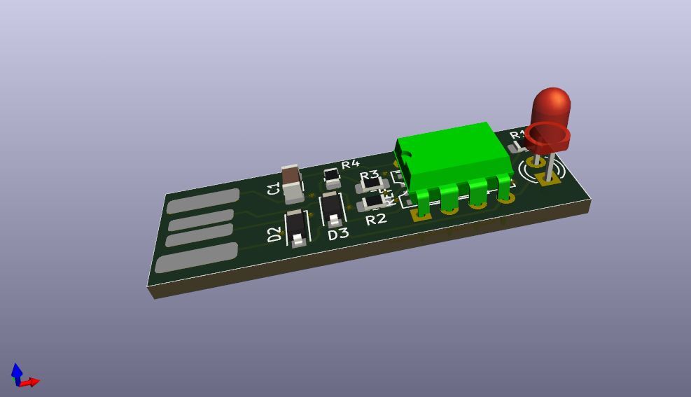
3D visualization of finished PCB design with component models and board shape
Reflection
This tutorial provided hands-on experience with KiCAD EDA tools and introduced the requirements for designing embedded microcontroller systems. Key takeaways include understanding the complete workflow from schematic to fabrication-ready files, differential pair routing for USB interfaces, and the importance of checking Fab Lab design rules (0.4mm trace/clearance) early in the layout process. Learning to work with the Fab Lab inventory system ensures that future designs can actually be fabricated and assembled in the lab without component availability issues. This foundational knowledge prepares me for designing custom embedded systems using standardized components.
Note: This assignment documentation website was created with assistance from Cursor AI.
Note: This assignment documentation website was created with assistance from Cursor AI.
Attachments
Links