04. ELECTRONICS (PCB) DESIGN
04
01
02
03
00
GROUP WORK
Softwares: KiCAD, SnapMagic Devices: Oscilloscope, Voltmeter
Files: Class KiCAD Repo, RFID Antenna

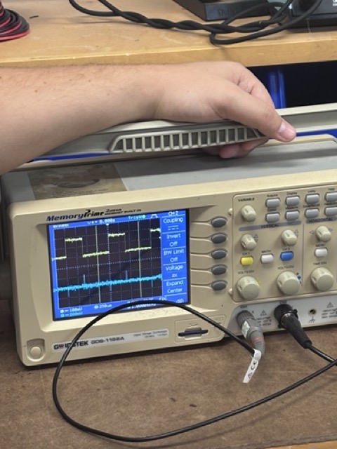
We met with Gert and looked at a few PCBs and used the oscilloscope to see the change in voltage over time! It worked on uncharged boards as well, and had zooming capabilities and basic graph modifications. Voltmeters also help to see if your electrical piece is getting enough charge.

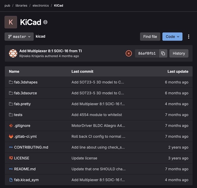
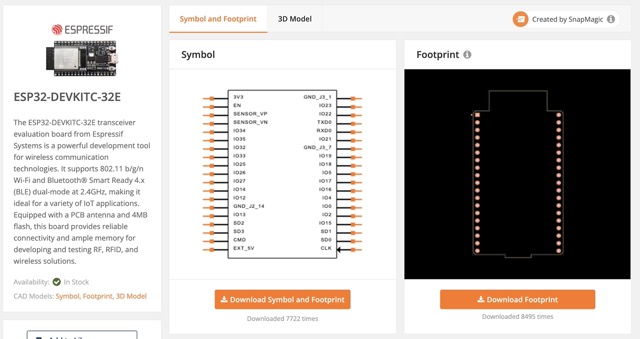
Then, I downloaded KiCAD and downloaded the class repository of parts/components for mental ease. For parts not listed, I used SnapMagic to find the KiCAD symbol and footer files It was also extremely nice to be able to quickly view the data sheets before making decisions about pins.
To start, I thought of some board ideas, the first being a PCB for my thesis project, the Kitchen Cosmo, and a PCB for my final project idea for this class, a Tarot Tutor! I laid out the components and figured my thesis work would be a bit more tedious due to the amount of components. So to start, I took another look at the electrical components for the Tarot Tutor.
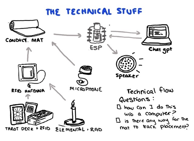
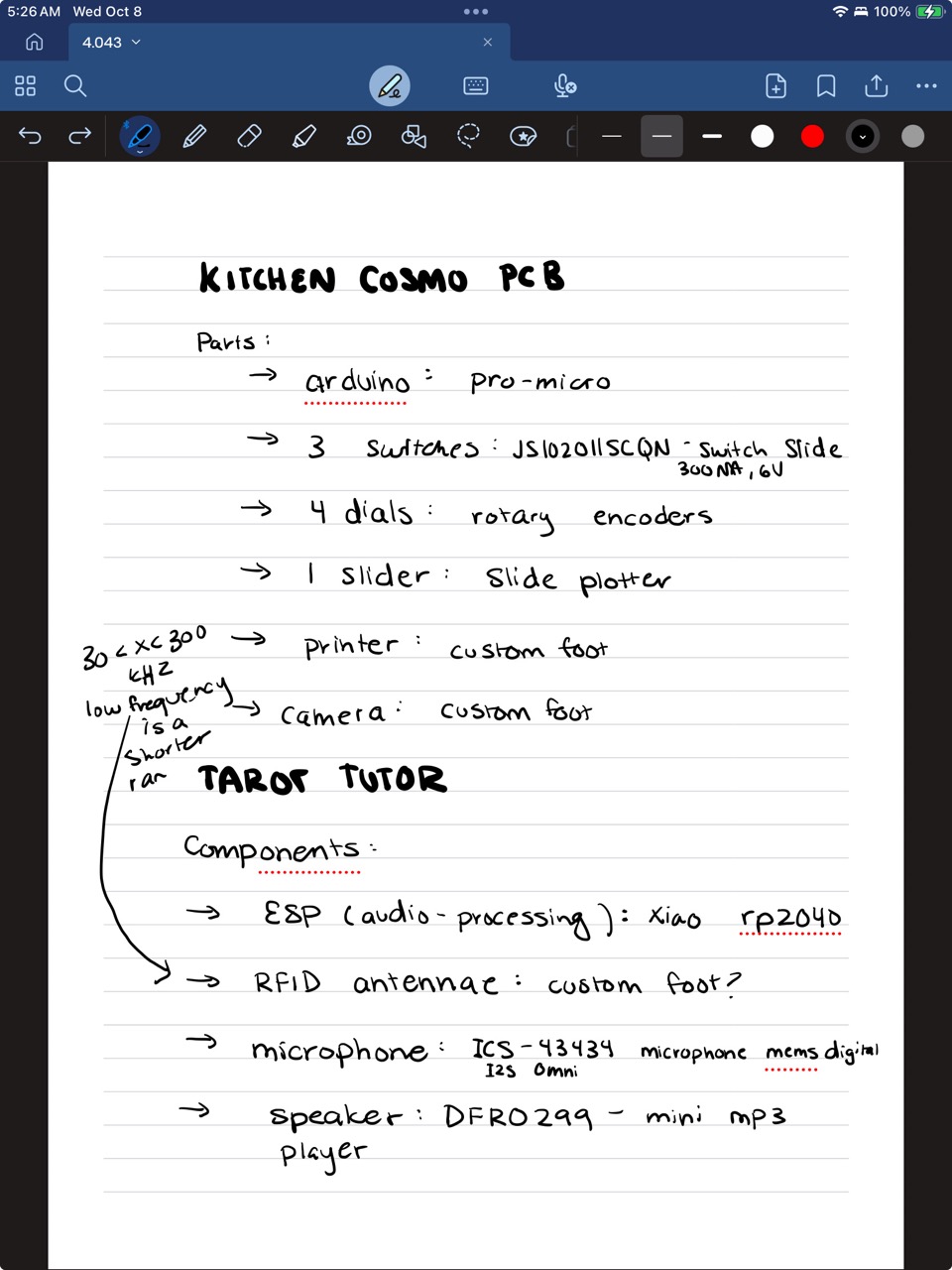
I made this sketch for my final project, and for this assignment I wanted to learn more about how to set up the technical flow. I don’t have experience working with RFIDs, so I had to do a little research on how they work to figure out the components and which set up would be the best for my project.


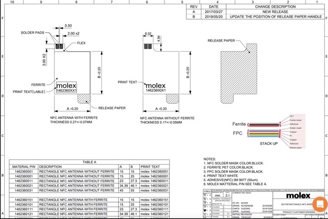
The data sheets surprised me a bit when looking for RFID antennas, there wasn’t an exact standard format. Some sheets were just product specs, others included descriptions for the type of antennae and graphs for sensor/radio wave perception tests. From this, I figured using a low frequency RFID antenna might be best for my Tarot Tutor mat so that the mat does not accidentally engage with and interpret cards that are just mid shuffle or still in the deck.
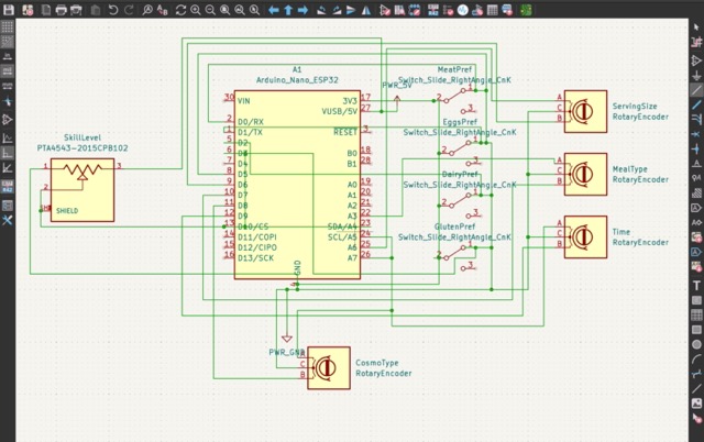
First, I started with the schematics and class KiCAD repository made things so much easier because I could just look up the exact component from the table that I wanted to use and instantly have the symbols for it. I think the only components I had issues with was the RFID antenna, because they only had a singular pin so I wasn’t quite sure how to connect it to the circuit, and the speaker. Since the mp3 player component had an audio output pin, I thought maybe I should attach an actual speaker to it? For this design, I really didn’t pay a close attention to having clean wiring, but I realized in the next part that it’s important to be able to see exactly which pins components are attached to. I also liked that this schematic environment lets me focus in on the actual circuit, instead of the overall layout of the board. I think I’ll throw up if I ever have to make my own components though...
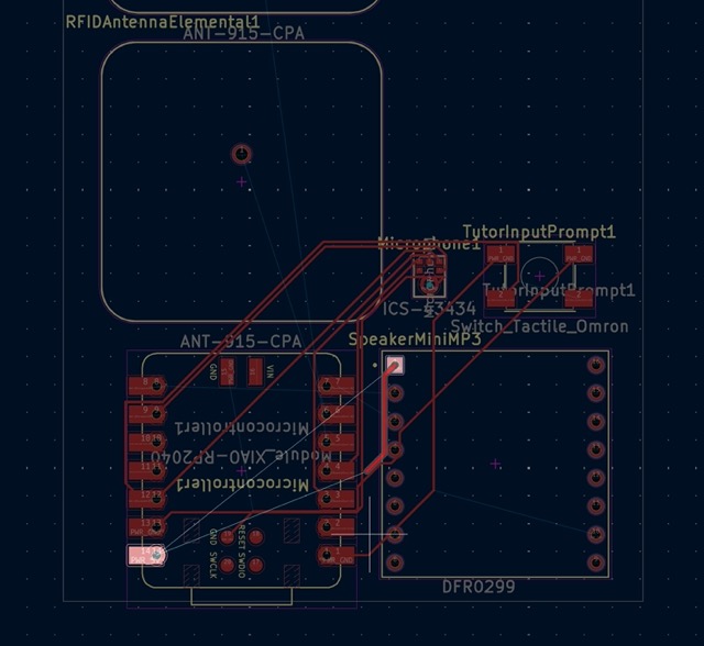
Moving onto the PCB editor, this step was fairly simple because I didn’t have many components, but I could definitely see it get challenging with a lot of components (see later). In this step it’s also important to make sure files and locations and labeled properly for the foot prints. This process kind of reminds me of MasterCAM.
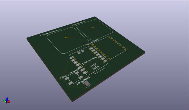
Finally, I looked at the board rendered, and although many of my parts did not appear, it was cool seeing my board in 3D. I also exported it as a Gerber file!
I also tried to make an extra PCB Design for my thesis, but I was super sleepy so I didn’t get tooo far, but I learned some things about modeling with many components. ORGANIZATION IS KEY!!!!! I was getting lost in my wires in the schematic because I wasn’t combining enough wires and spacing things smartly.
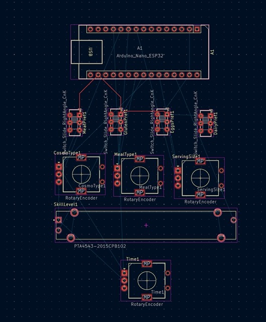
I finished up with the schematics and moved onto the PCB editor aaaaaaand quickly gave up trying to wrap my head around how to get this together without having multiple layers. ;o;
KICAD & SET UP
TAROT TUTOR PCB DESIGN
KITCHEN COSMO PCB DESIGN


(ESP for wireless connection and perfect for RFID (has an attached “PCB antenna”))
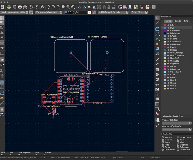
Routing fail!! At first I didn’t want to figure out layering, but I guess I’ll need to ;-;
After some moving some things around, I finally found a way to route everything in one layer.
RFID Description - Data Sheet 2 (the one I used)
RFID Specifications - Data Sheet 1 (the one I used)


TRIALS & TRIBULATIONS
LESSONS LEARNED
Overlapping routing/trying to figure out the best path for the final cuts took a few tries... The best solution would definitely be to figure to cut on multiple layers, and I got halfway through figuring it out before I had an issue connecting the wire to the correct pin.
Keeping organized in terms of components and wires.
Use SnapMagic to find KiCAD files, as well as some where to buy parts!
There’s many ways to do an RFID, it would be smart to order an antenna and tag to start testing for what would work best soon
Previous to this assignment, I had always thought that PCB design was extremely difficult because of all the steps and necessary file downloads, but I feel like it’s been demystified for me partially! :D
