Week 5: Electronics Design
Assignment
- group assignment:
-
[done] use the test equipment in your lab to observe the operation of an embedded microcontroller
- individual assignment:
-
[done] simulate a circuit
-
[done] use an EDA tool to design an embedded microcontroller system using parts from the inventory, and check its
design rules for fabrication
Group Assignment

Please see this link for my group
assignment (Session 1). Just wanted to note that I had a TON of fun working with my classmates on these skills.
Thanks, Eitan and Miranda, for writing up all the notes (see above) and taking great pictures!
Individual Assignment
After a bit of brainstorming (see below), I decided to use this week’s assignment as an opportunity to understand
some of the components on this Giant Garbage PCB (GGPCB) I found in the heap outside of the Mars lab. The board is
labeled: “Acoustic Receiver and Quadrature Demodulator” and was made in 1998 (the year after I was born).
I noticed that there are a number of repeating sub-units on the board which use the same ICs (see below). After
looking through the datasheets for a few of them, I became fascinated with the MAX262, a programmable active filter.
Essentially, by changing the input signal to this IC, you can change the parameters of the active filter circuit. A
lot of the datasheet was gibberish to me at the start of the week, so I decided to take a step back and build up to
understanding how it worked.
Big idea: Design a circuit board which demonstrates the function of multiple low-pass filter types. Simulate a
microcontroller generating a variety of sin wave input signals and view what happens to these signals after they go
through each filter.
- Passive
- Active
- Filter using Op Amp(s) TLV365DBVR
Components on the GGPCB
- 93A0FFK - SN74LS240N (TI)
- AD -823AN-9776
- Dual, 16 MHz, Rail-to-Rail FET Input Amplifier
- https://www.analog.com/media/en/technical-documentation/data-sheets/AD823.pdf
- MAXIM-MAX262BCNG
- Microprocessor Programmable Universal Active Filters
- https://www.mouser.com/datasheet/3/1014/1/MAX260-MAX262.pdf
- check out this application
note from a college team
- SSM2141 (850 G925050)
- High Common-Mode Rejection Differential Line Receiver
- https://www.analog.com/media/en/technical-documentation/data-sheets/SSM2141.pdf
## Research Before diving into circuit design, I really wanted
to understand the fundamentals of these different types of
circuits. A friend of mine gave me a copy of “Practical
Electronics for Inventors” a while back, and I’d perused it,
but never really tried to use it before. This seemed like the
perfect opportunity! ### Notes from “Practical Electronics for
Inventors” (link)
- Passive Circuits (Scherz and Monk, p.664)
- work best for frequencies from 100 Hz to 300 MHz .
- steep attenuation requires more inductors/capacitors
- must account for source and load impedances
- Active (Scherz and Monk, p.664)
- can handle very low freq. signals (approaching 0 Hz)
- can provide voltage gain (amplification)
- no good for high frequencies (above ~100 kHz)
- A note on filter types (Scherz and Monk, p.670)
- main filter types are Chebyshev, Bessel, Butterworth
- Butterworth are the most popular
- flat response in middle region
- easy to make
- less strict component tolerances
- Issue with Butterworth and Chebyshev
- they garble modulated signals because they add varying
delays based on freq
- this is where bessel filters are best
- they have less steep attenuation, but delay all signals by same amount of time
- this is not relevant for my application, so a butterworth should work nicely
- Switched-capacitor IC’s (like the ones on my trash board)
- Instead of using external resistors to program the desired
characteristics, you do so by sending it a clock signal of a
particular frequency
Designing an oscillator for input wave form
- NOTE: decided to just use the DAC output of the SAMD21
instead of building an oscillator from scratch.
- Analog
- Relaxation oscillator
- Wien-Bridge and Twin-T Oscillator (p.693 of Practical
Electronics)
- can achieve 1-5 kHz frequencies
- Check out resistor DAC ladder on p.885 of practical
electronics
- able to achieve frequency range from 60-5 kHz
- Digital
- Look back into SAMD21 DAC output
- should be able to produce up to 175 kHz Sin waves
(according to data sheet) ### Designing Filters
Designing all filters for a f_db3 = 500 Hz and -60 dB of
attenuation at 2500 Hz
Single Stage Passive
- Follow instructions on page 210 of Practical
Electronics.
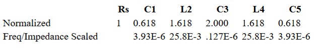
Multi Stage Analog Filter
- Following the instructions beginning on 667 of Practical
Electronics, I arrived at needing to build a 5th order
butterworth filter (pi configuration since assuming/trying to
match impedance of output and input)
- to perform impedance scaling, we must know the load
impedance of the circuit. But these circuits aren’t driving
anything, so what is the output impedance?
- woahhhh just founded the book online
- I think this means that I should be terminating my filters
with a dummy load that matches the input impedance of the
circuit.
- So, what is the input impedance of the circuit? I imagine
this is equal to the output impedance of the MCU’s ADC pin.
Let’s find that.
- This (of course) was non-trivial to find. The SAMD21
datasheet doesn’t specifically mention impedance with respect
to the DAC, but it does say:
- “High-drive capabilities” -> which implies low
impedance
-
and, the block diagram (see below) represents the output with an output driver op-amp (further indicated lowimpedance)
-
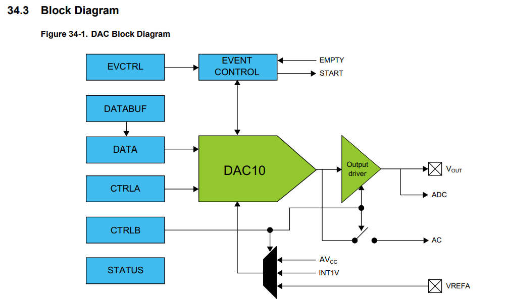
- looks like I’m not the only one with this problem link
- the best I can find in the datasheet is “The DAC output
buffer provides a high-drive-strength output, and is capable
of driving both resistive and capacitive loads.” with no
specification of the size of these loads
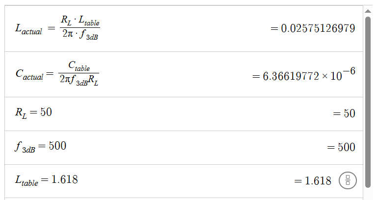
- bearing all of this in mind, let’s just model this as a 50
ohm impedance for now and see how it works. Okay, using
formulas listed on p. 669 to perform scaling:
- e.g.
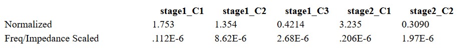
Multi Stage Active Filter
- As was true for the above, I will need a 5th order filter,
although the table values are structured differently (see
Table 9.2 on p.676). Let Z = 50 ohm
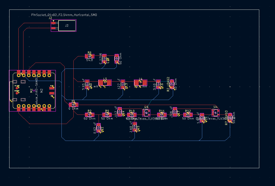
Getting into KiCAD
Although I’ve used KiCAD before, I’ve never taken a circuit from an idea all the way through PCB design. This was a really helpful exercise! I am using KiCAD version 8 and found the KiCAD docs to be immensely useful. Essentially, I followed the steps outlined there to make my schematic and then generate a PCB. The notes below largely capture moments when my experience deviated from what I had expected to see while following the documentation
- Generating a Schematic
- Ran ERC (rules checker) and learned the following lessons:
- all disconnected pins need to be designated as "nc"
- all power inputs will need to be labeled with a PWR_FLAG
- Generating a PCB
-
set design rules according to this site except I made minimum track width 0.4mm as discussed in class
-
Was feeling pretty good, then ran design checker and BAM whole bunch of errors
-
Most of them were because I needed to add vias such that my back traces were actually connected to the pads on the front. Just because a trace terminates at the same position as a pad does not mean that it is connected (see below).
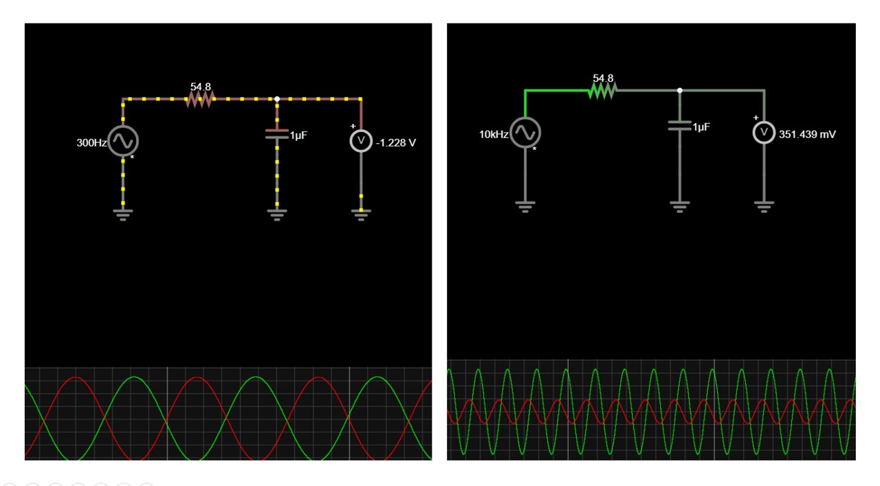
Running Simulations
At first, I tried to run my simulations in KiCAD, but I was having a lot of trouble getting that working. Ultimately, I went to office hours and Miranda taught me how to use https://www.falstad.com/circuit/avr8js/ to simulate my circuits. I found this to be a much more straightforward process as it is pretty much drag and drop.
Circuit 1: Passive Single Stage Low Pass Filter (link)
Attenuation was minimal for low frequencies, and significant attenuation at higher frequencies (as expected)!
Circuit 2: Two Phase Passive Circuit (link)
Wow! Using a multistage passive filter made a huge difference in attenuation.

Circuit 3: Multi Stage Active Filter(link)
I’m not totally sure what the issue is with this filter, but it seemed like it did NOT want to let low frequencies pass. More to explore for another time!

Acknowledgements
-
Shout out to Miranda for teaching me how to use AVR simulator and obsidian.
Return to Home Page