This week we explored the world of electronics design and fabrication.
I learned how to create custom circuit boards using KiCad and then sanity-check behavior with simulation. Next week we’ll solder and mill to see them truly take shape. As a physicist, I’ve always found PCB design a bit intimidating; the big win this week was simply not being afraid of the PCB anymore.
Ok—let’s jump in.
The work split into a group assignment and an individual assignment.
We used the Architecture Lab test equipment to observe the operation of a microcontroller and documented the process here: arch lab week 5.
Goals:
I scoped my individual work toward my final project: earring–earphones. For a wearable, I want the board small and “jewelry-friendly,” with:
My final project aims for earrings that double as wireless earphones, ideally with kinetic energy harvesting to assist charging. This week I built a first circuit foundation toward that goal.
Power management is the hardest piece, especially as a newcomer, so I began by getting a simple, working platform before shrinking it.
Constraints: tiny footprint, capacitive touch inputs, Bluetooth for wireless audio, and a path to battery charging.
The Seeed XIAO ESP32-S3 fits well: compact, BLE 5.0, and enough GPIO for touch + RGB + I²S. I also explored piezoelectric energy harvesting (see milestones) to capture motion energy from the earrings.
| Part / Board | Core / Family | Form factor | Dimensions (mm) | GPIO | Bluetooth | Other notes | Ref |
|---|---|---|---|---|---|---|---|
| Seeed XIAO ESP32-S3 | ESP32-S3 (Xtensa) | Module | ≈ 21 × 17.8 | ~11 | BLE 5.0 | Tiny; Wi-Fi 2.4 GHz; deep sleep support | Wiki |
| Seeed XIAO ESP32-C3 | ESP32-C3 (RISC-V) | Module | ≈ 21 × 17.5 | ~11 | BLE 5.0 | Wi-Fi 2.4 GHz; low power; onboard charger | Wiki |
| Seeed XIAO SAMD21 | ATSAMD21G18 (M0+) | Module | ≈ 21 × 17.8 | 14 | No | Arduino-friendly; external BT needed | Wiki |
| Seeed XIAO RP2040 | RP2040 (dual M0+) | Module | ≈ 21 × 17.8 | ~11 | No | Great toolchain; no radio | Wiki |
| Raspberry Pi Pico W | RP2040 (dual M0+) | Board | 51 × 21 | 26 | BLE 5.2 | Wi-Fi 2.4 GHz; larger footprint | Product brief |
From this comparison, the XIAO ESP32-S3 stood out. First step in KiCad: add the XIAO symbol and footprint to the schematic.
In the PCB editor:
TestPointTestPoint_Pad_D6.0mm, D8.0mm, or D10.0mm)I first tried editing only in the PCB editor and hit “Update Schematic from PCB” limits. KiCad’s source of truth is the schematic:
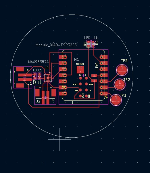
Core blocks: XIAO ESP32-S3, RGB LED (common-anode + 3 resistors), three capacitive touch pads, optional MAX98357A I²S amplifier, JST-PH battery input, and decoupling capacitors.
I labeled I²S nets (DIN, BCLK, LRCLK) and placed decouplers close to VDD pins. Remember: define everything in the schematic first.
PWR_FLAG on GND, VBAT, 3V3SD_MODE/GAIN_SLOT and labeled I²S nets carefullyAfter a few iterations, ERC was clean (aside from the expected exposed-pad note).
Seeed_XIAO:Seeed_XIAO_ESP32-S3
Update PCB from schematic → place components. Amp near speaker connector; keep OUTP/OUTN wide (~1 mm). Place decouplers within a few mm of VDD with short GND returns. Ground pour both layers + stitching vias. Touch pads on the edge for usability.
First pass flagged seven items (courtyards, silk over edge, a couple of missing nets). Fixes:
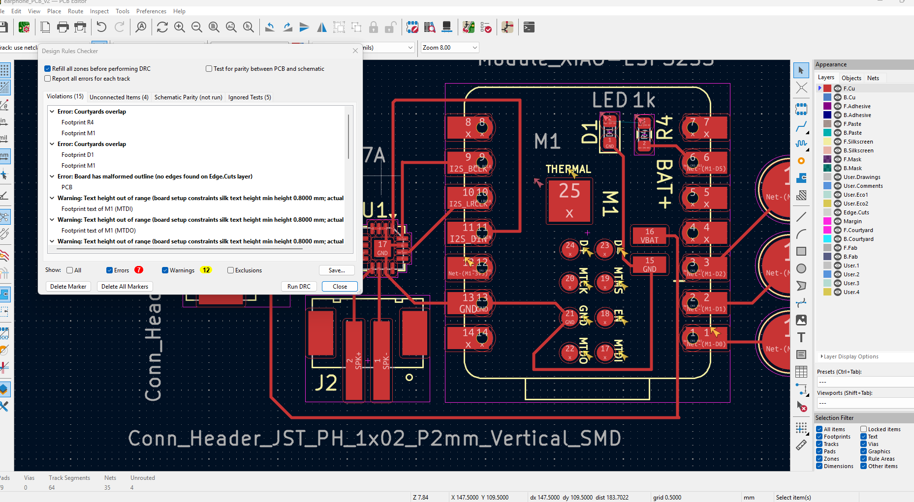
Edge.Cuts outlineAfter fixes, DRC ran cleanly.
Full ESP32-S3 + I²S isn’t practical to SPICE, so I split validation:
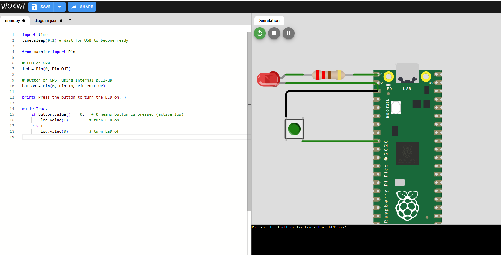
Note: I initially assumed common-cathode and wondered why the LED seemed “always on.” Switching to common-anode logic fixed it.
For an earbud driver, I chose the MAX98357A I²S Class-D amplifier:
References: Adafruit breakout · Datasheet (Digi-Key)
Battery: I broke out a 2-pin JST-PH for a 1-cell LiPo so I can add charging/power management in a later rev.
Mid-work, I had an unexpected power outage and a couple of computer crashes. One crash cost me a chunk of unsaved KiCad edits (ouch). The silver lining: better save discipline and using ERC/DRC early to recover faster.
Explore the files:
Tip: right-click → “Save link as…” if a download doesn’t start.