Week 6 — On Painting with Copper
As part of the group assignment, our section also submitted a PCB design to an external board house.
overview
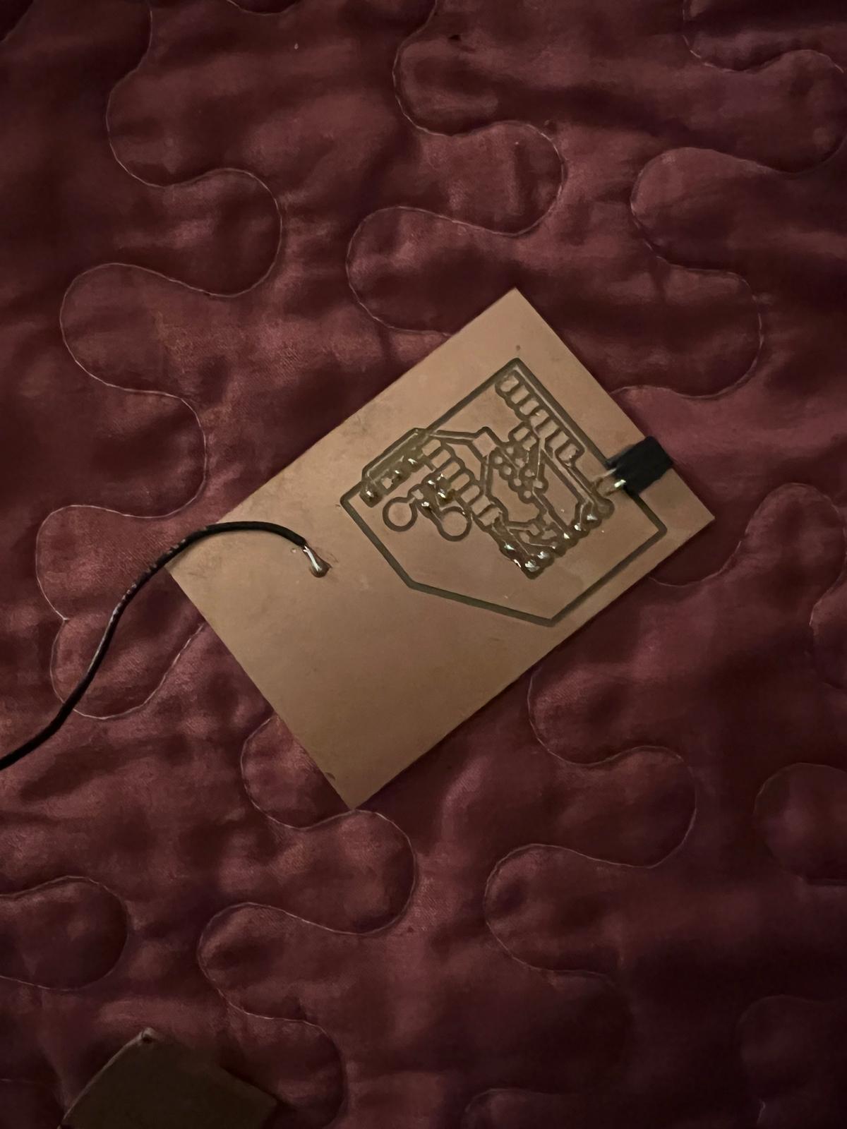
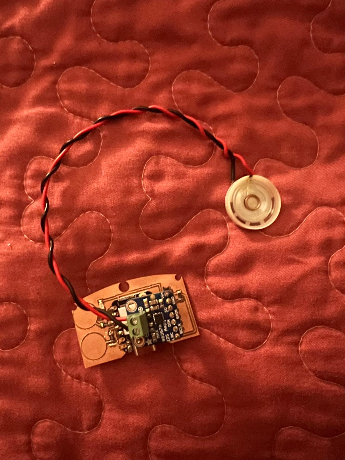
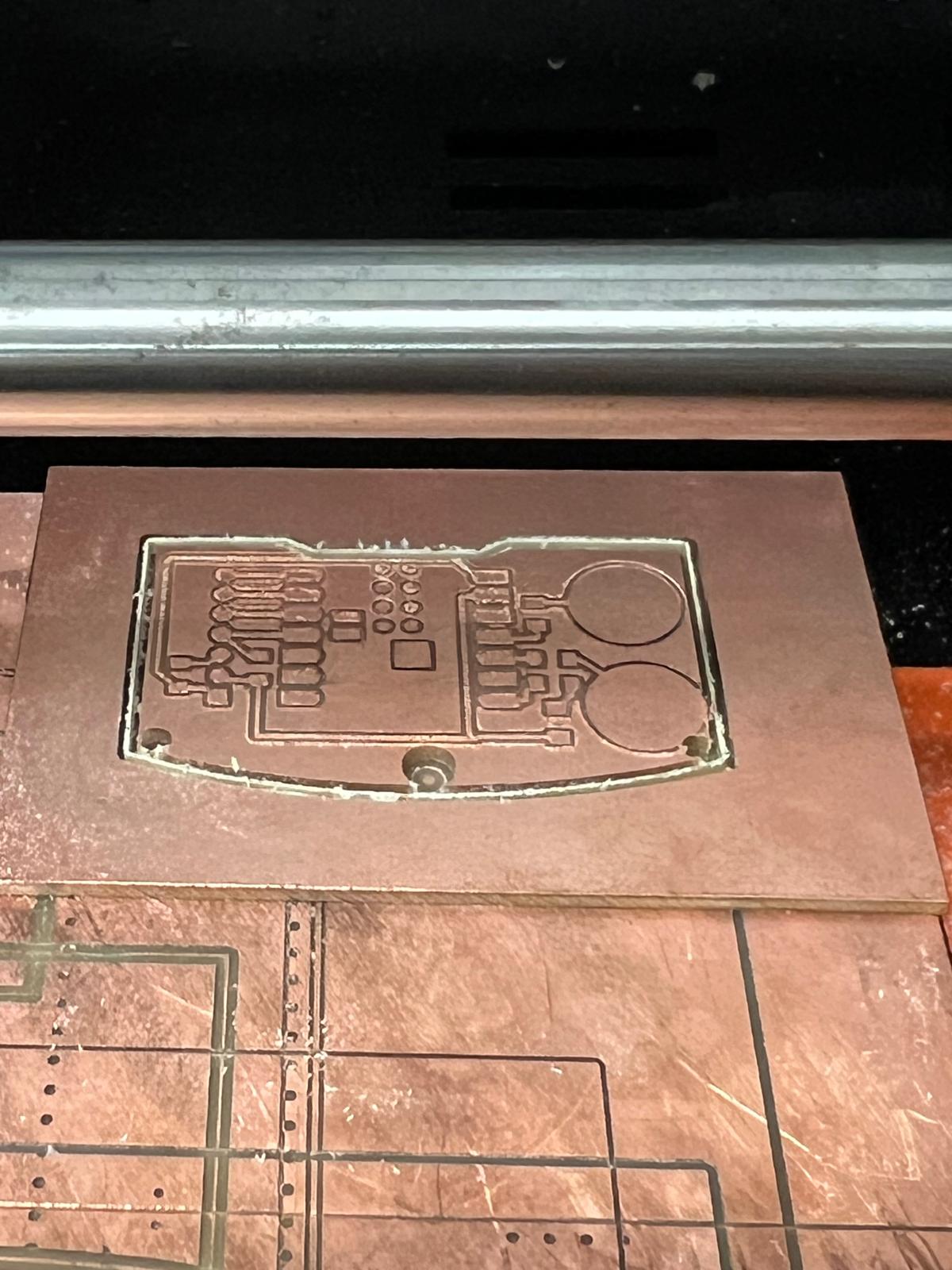
This week I continued the “earphone earrings” dream. I started bold, then realized the first version used a part that isn’t in the lab inventory (oops). So I pivoted to a breakout‑friendly design: an Adafruit MAX98357A I²S amp and a discrete 8 Ω speaker. My custom board handles power, connectors, and shiny copper capacitive pads. Copper‑ation, if you will.
pivot & resources
I read around on earphone PCB layouts and community projects to sanity‑check the new plan: earphone PCB overview · WirelessHardware repo. The goal was to minimize custom analog while still learning PCB layout on a wearable form factor.
parts & links
| Item | Link | Notes |
|---|---|---|
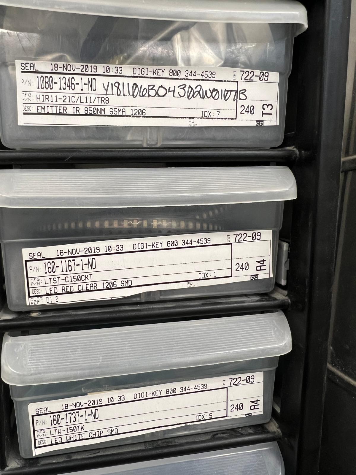
| I²S amplifier breakout (MAX98357A) | Adafruit 3006 | DAC + class‑D. Inputs: BCLK / LRCLK / DIN. Output: SPK± (don’t ground SPK−). |
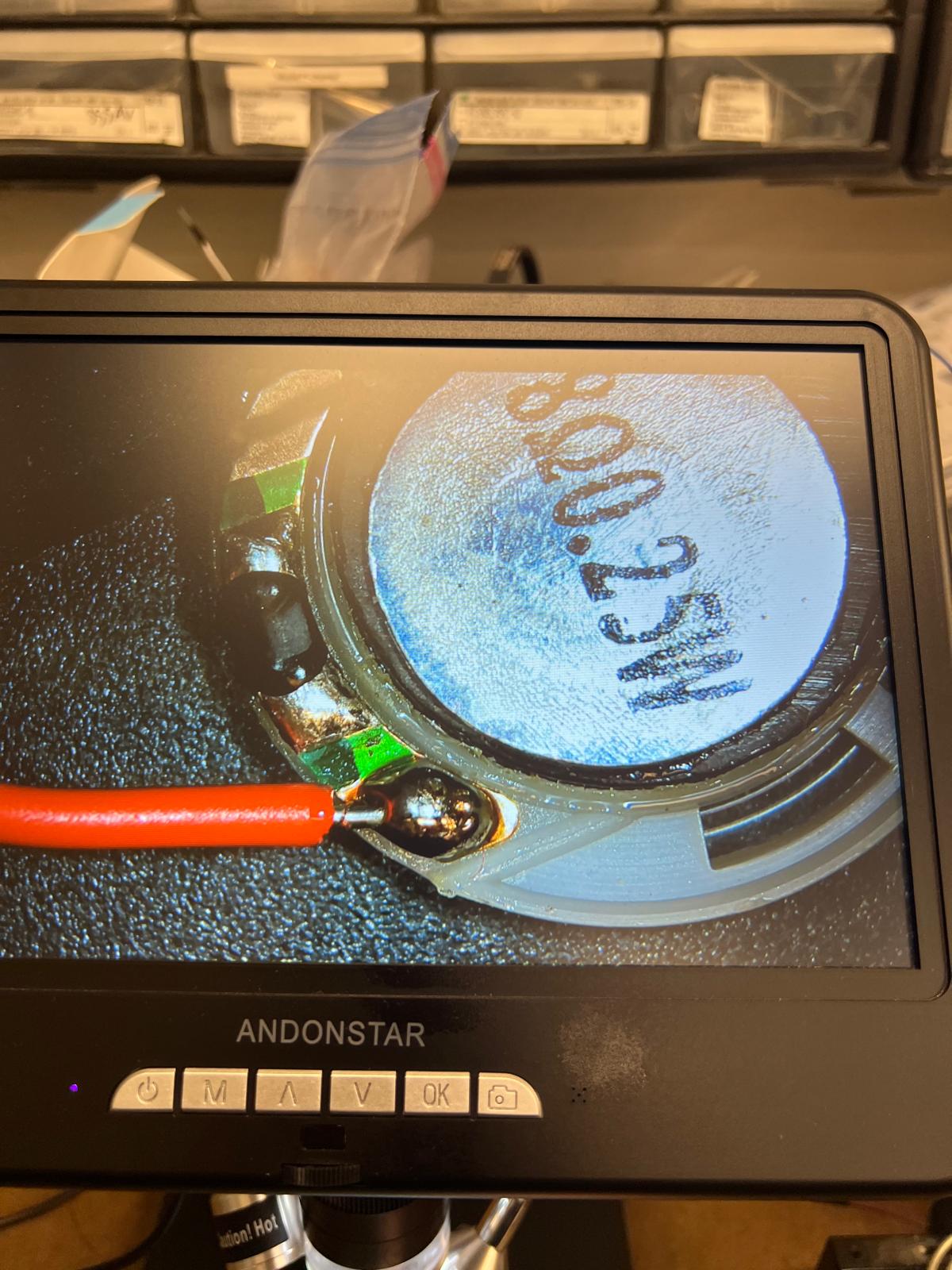
| 8 Ω speaker | Mallory PSR‑23F08S‑JQ | Panel‑mount; wire directly to breakout’s SPK± terminals. |
| MCU | Seeed XIAO ESP32‑S3 | I²S output; touch‑capable GPIOs for the capacitive buttons. |
| Headers / sockets | 1×7 female socket (2.54 mm) | Matches the breakout’s 7‑pin header footprint (I originally thought 8, ha!). |
technical design summary
ESP32‑S3 doesn’t have a true DAC. I wanted clean audio without wrestling PWM filters, so I picked
the MAX98357A:
the ESP32 sends I²S (BCLK, LRCLK, DIN) and the breakout does the DAC + class‑D part
to drive the 8 Ω speaker directly.
breakout header mapping
Adafruit‑style 7‑pin order (left→right): LRC, BCLK, DIN,
GAIN, SD, GND, VIN. I used a 1×7 female socket so the module with male pins can plug in.
wiring plan
- Power: VIN ↔ XIAO 5 V/VBUS; GND ↔ board GND plane.
- I²S: LRC ↔
I2S_LRCLK, BCLK ↔I2S_BCLK, DIN ↔I2S_DIN. - SD/MODE: default enabled via pull‑up (or drive from a GPIO for mute).
- GAIN: left floating for default gain (strapable later).
- Speaker: solder leads directly to breakout SPK+/SPK− (differential).
capacitive buttons
Two big copper pads → touch‑capable GPIOs, each with ~220 Ω–1 kΩ series resistor for ESD/RF sanity. Firmware plans: Play/Pause (tap) and Volume (tap=up; hold=down).
sd/mode quick reference
- SD < 0.16 V → shutdown
- 0.16–0.77 V → stereo average (default)
- 0.77–1.4 V → right only
- > 1.4 V → left only
schematic & pcb notes (what I tried & why)
- Single GND plane so return currents aren’t playing hopscotch; both XIAO GND pins on the same net.
- Added a
PWR_FLAGon 5 V so KiCad ERC knows USB can power the board. - Routed the I²S bundle short and parallel; kept the touch traces away from the speaker loop.
- Placed a copper keepout under the touch pads to boost sensitivity (air > FR‑1 here).
// example pins (firmware bring-up)
#define I2S_BCLK  8
#define I2S_LRCLK 9
#define I2S_DOUT  10
// init I²S → generate a sine → scale by 'volume'
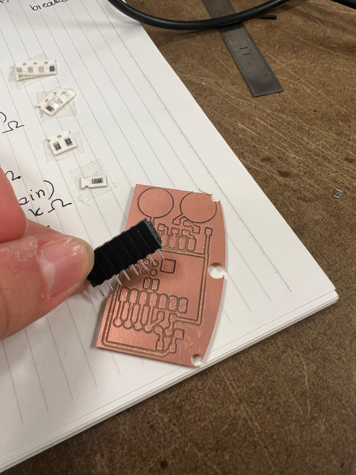
breakout footprint plan
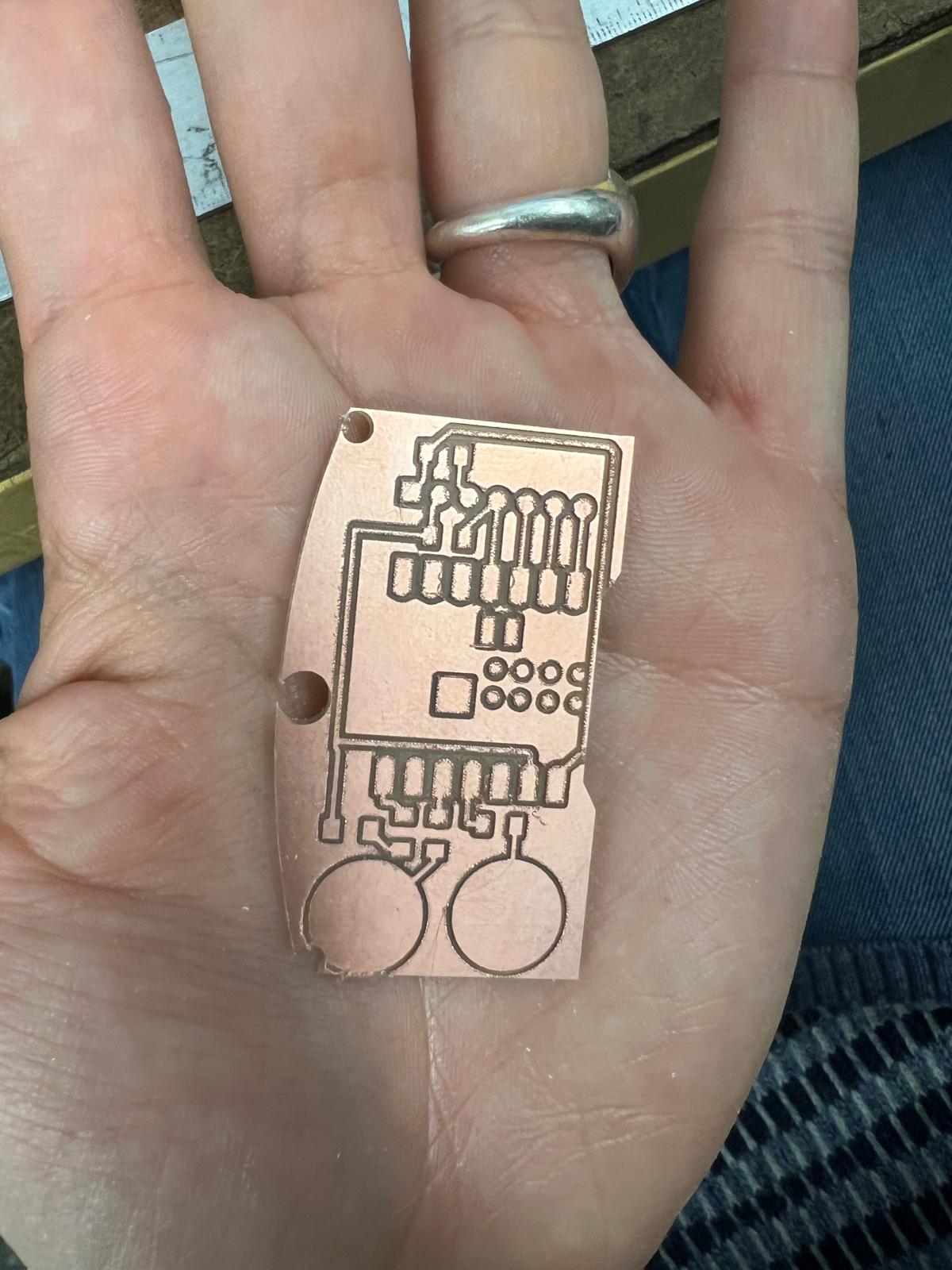
I first allocated 8 sockets (optimism!), then corrected to 7 to match the breakout. Labels mirror the breakout silkscreen to be future‑me‑proof.
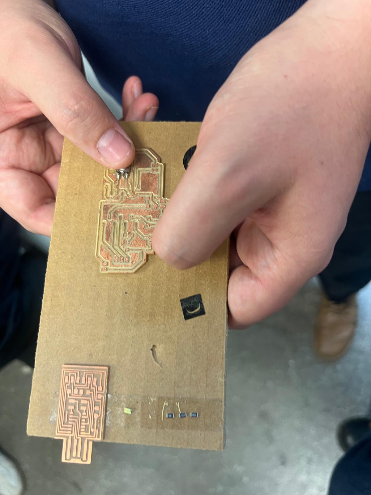
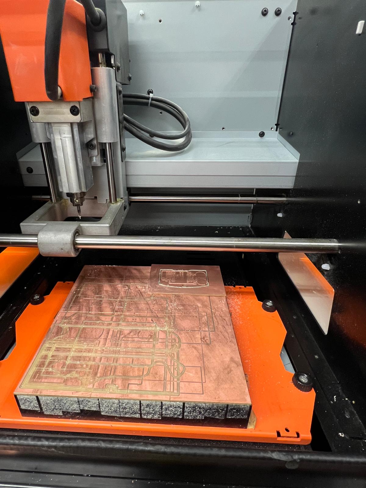
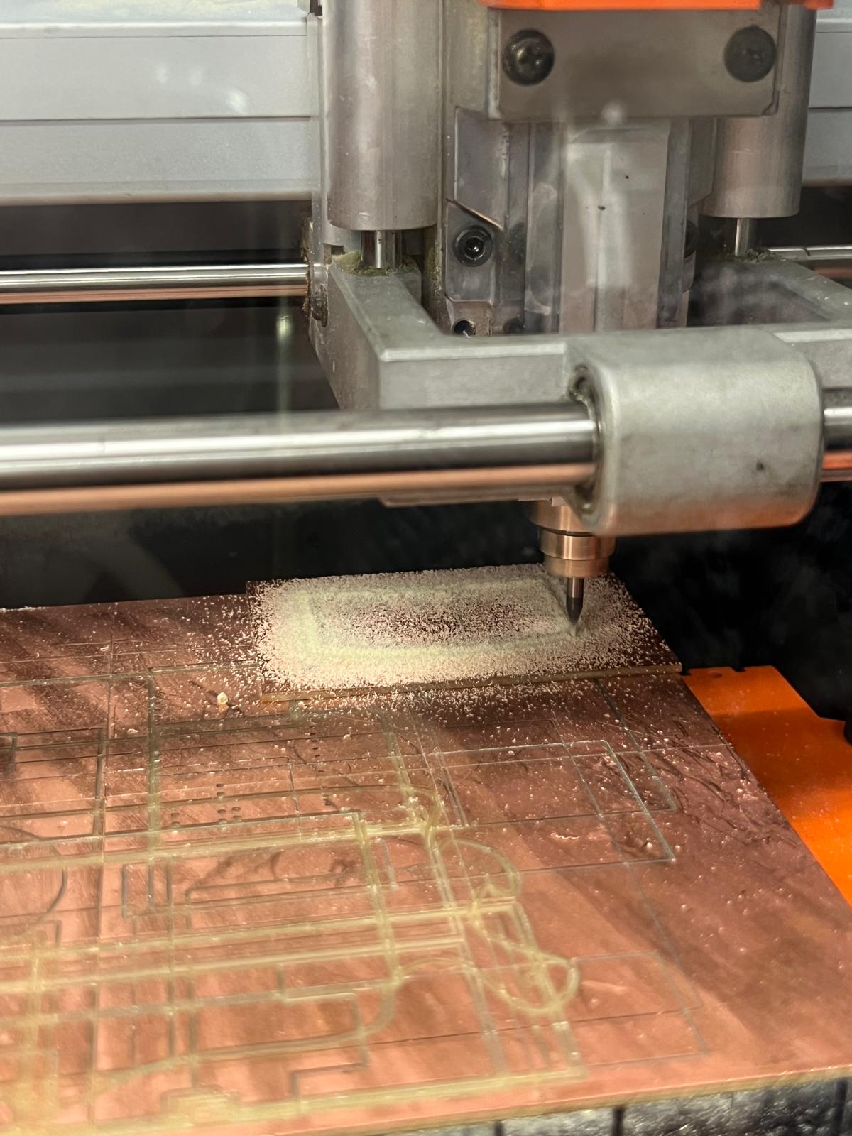
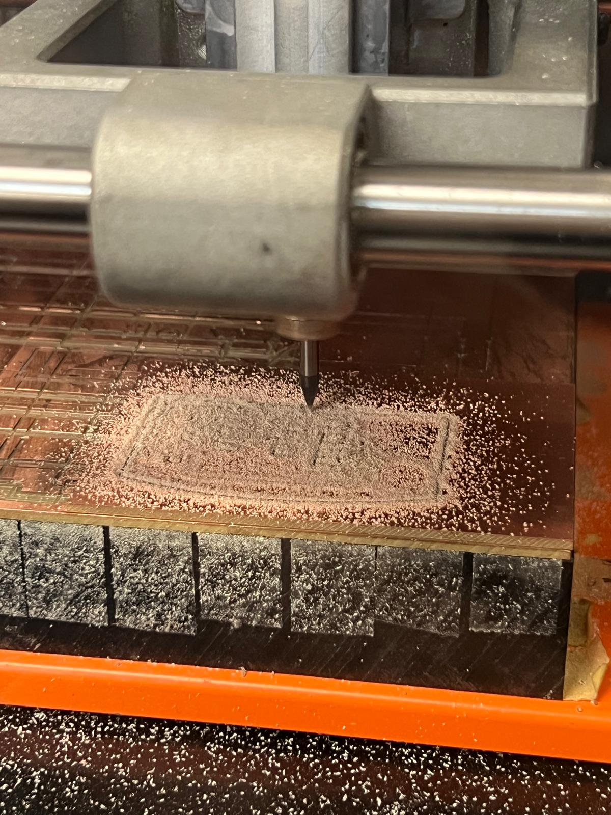
pcb iterations & mistakes
PCB v1 was a learning board. Things I messed up, and the fixes I shipped in v2:
- Blocked the XIAO’s USB‑C with components (facepalm).
- Traces too thin for milling → fragile isolation.
- Capacitive pads too small → shy to the touch.
- No copper pour → lots of skinny, sad traces.
Fixes: USB‑C keep‑out, wider traces/clearances, bigger pads, solid GND fill.
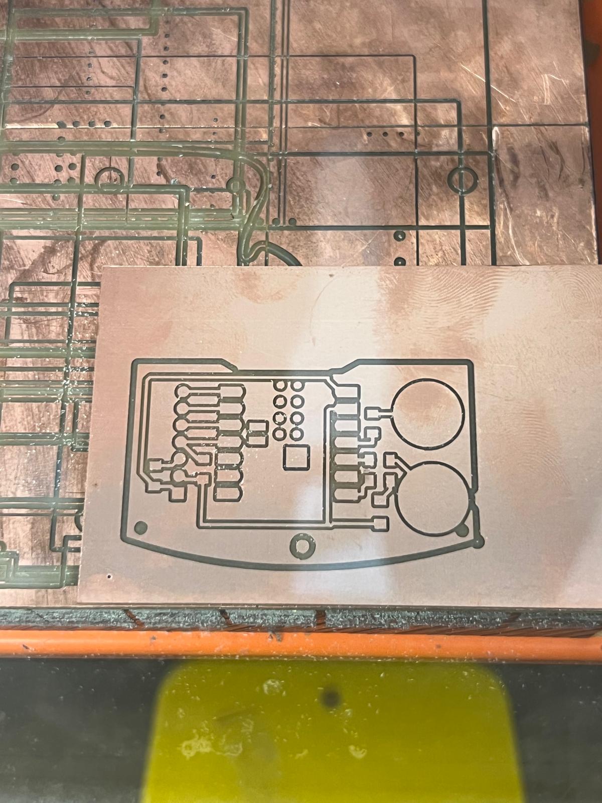
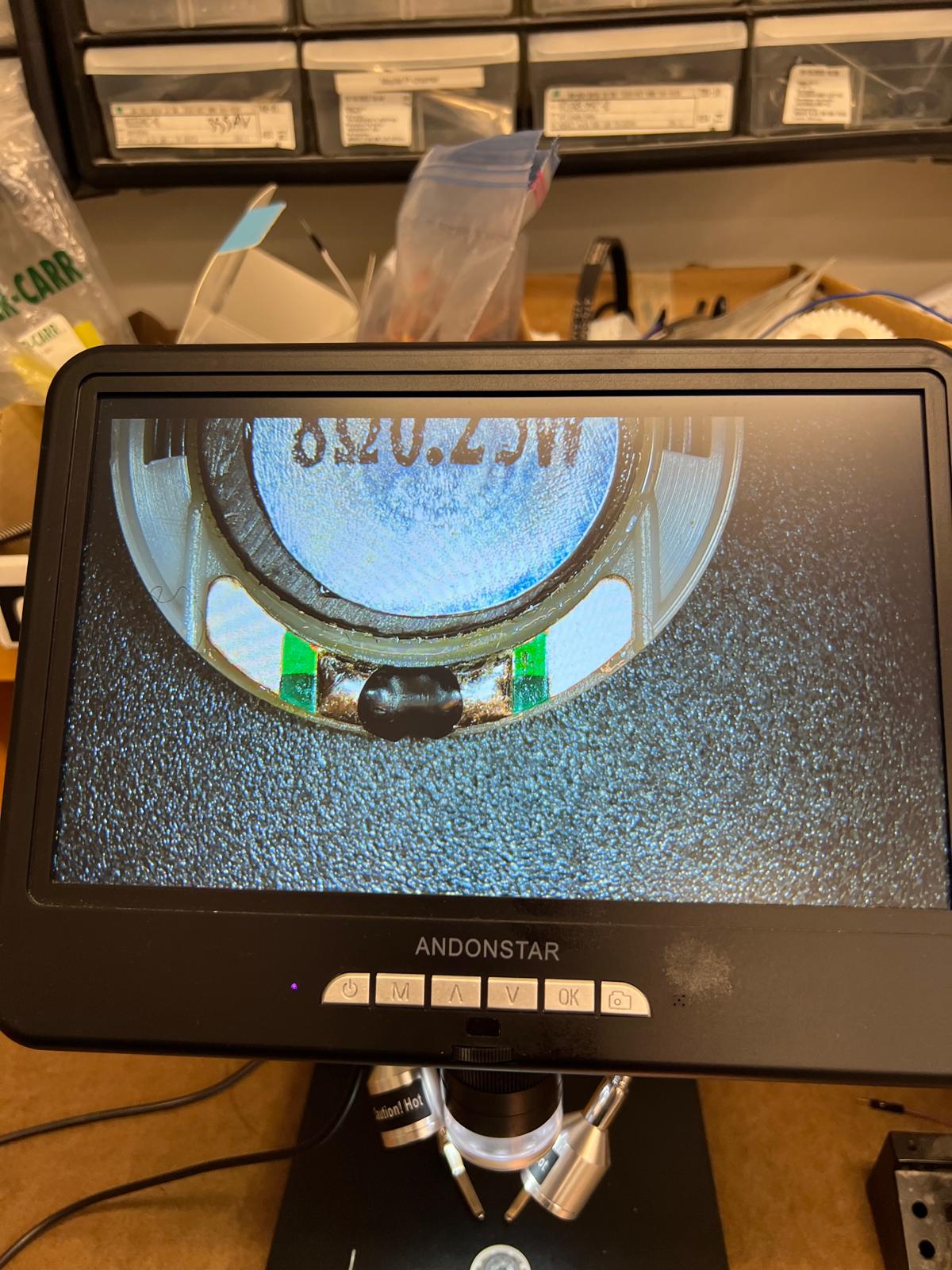
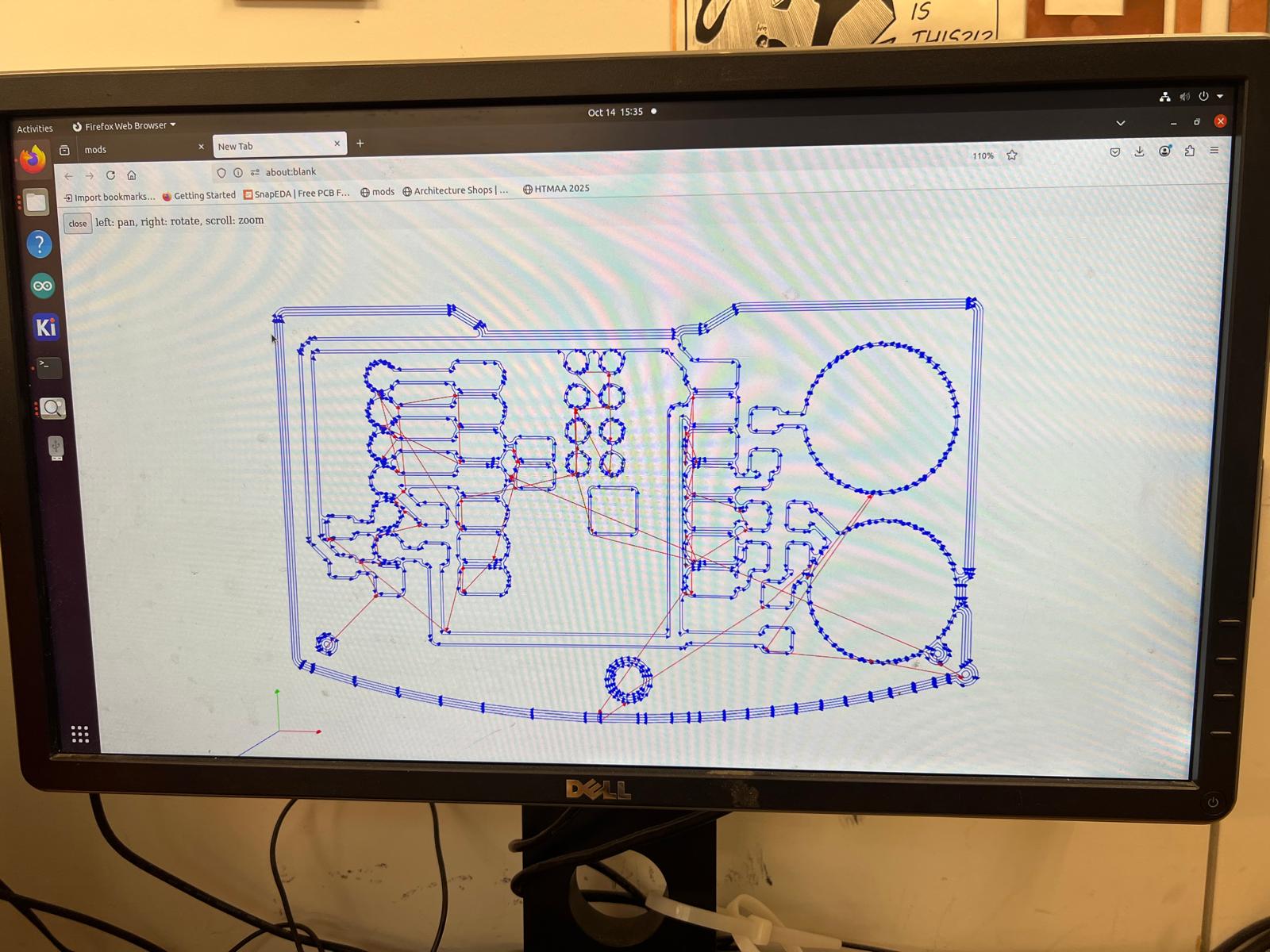
milling notes
Milling on the monoFab became the plot twist: ~30 min cuts + ~20–30 min setup/debug. One tiny fail can cost an hour, and lines form fast. Copper patience is a virtue.
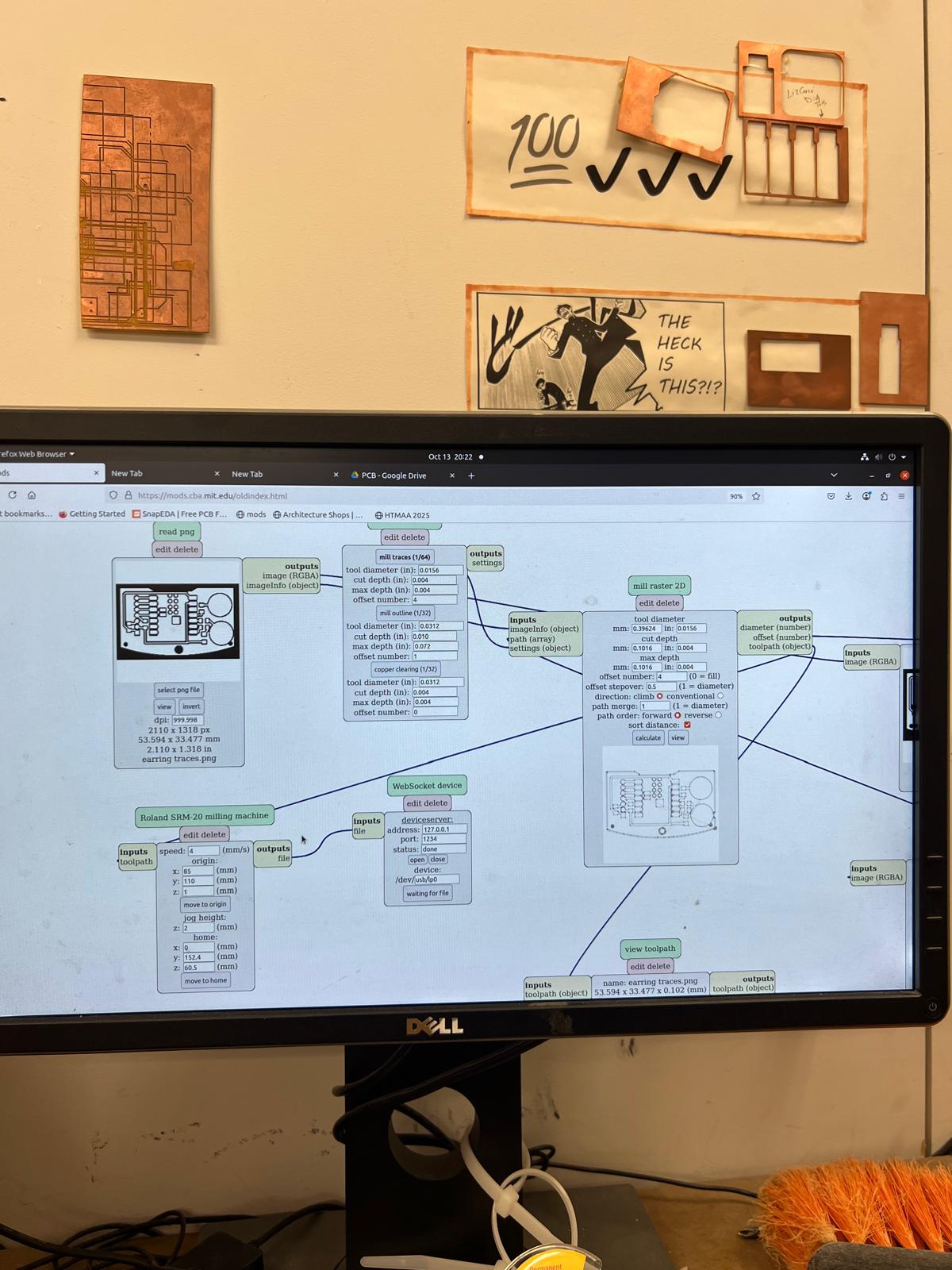
mods settings used for trace/outline jobs.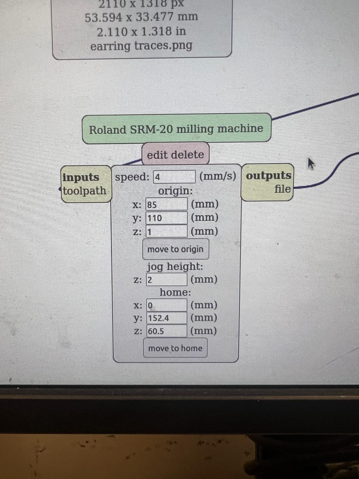
pcb-as-earring idea
Because jewelry! I added small edge‑cut loops so the board can hang like an earring. It looks fun; we’ll see how the FR‑1 edges hold up in the wild.
bring-up & testing
My plan was: continuity → power‑only → LED → touch → I²S wiring → audio. Here’s what I actually got through.
- Continuity/shorts: checked 5 V/3V3 rails, GND, headers, pads, LED net.
- Power‑only test: enumerated over USB‑C, no suspicious heat.
- LED sanity: wrote a tiny blink sketch to confirm GPIO mapping.
LED test code
First, verify the LED pin actually toggles. Simple, but catches wiring mistakes fast.
// Simple LED blink test for Xiao ESP32-S3
// Replace LED_PIN with the actual GPIO you wired the LED to.
// If you're using the *onboard* status LED, try LED_BUILTIN.

int LED_PIN = 8;  // change to your LED GPIO (or use LED_BUILTIN)

void setup() {
  pinMode(LED_PIN, OUTPUT);
  // optional: start LOW so you can see the first transition clearly
  digitalWrite(LED_PIN, LOW);
}

void loop() {
  digitalWrite(LED_PIN, HIGH);
  delay(500);
  digitalWrite(LED_PIN, LOW);
  delay(500);
}
…and then we got stuck
I hit a wall talking to the Xiao (uploads failing). Classic lab hour plot twist. Here’s what I tried before time ran out:
- Swapped USB‑C cables and ports; confirmed power and data (not charge‑only).
- Toggled board/port settings in Arduino (XIAO ESP32‑S3, correct COM, upload speed).
- Pressed BOOT/RESET combos to enter the bootloader.
- Disconnected anything on pins that could fight the USB/UART during upload.
- Checked continuity again on 5 V/3V3 and GND; no obvious shorts.
Still no luck within the time window, so I parked firmware and focused on documenting the hardware steps (this page!). Next week I’ll get it talking and then add the I²S tone test.
people & thanks
MVP: Aidan (Architecture shop) — monoFab whisperer. Huge thank you to Gert for coming in on his days off (Sunday & Indigenous Peoples’ Day) to support the Arch section.
next steps
- Fix the upload issue and run the I²S tone test with the MAX98357A.
- Map capacitive pads to play/pause + volume, then add LED color states.
- Stress‑test the PCB‑as‑earring mounting and iterate shape/finish.