This week I added an audio output path to my custom XIAO ESP32-S3 board: a tiny class-D amplifier driving an 8 Ω speaker. The focus was on hardware design—schematic edits, routing, power integrity, and fabrication—so I can program it next.
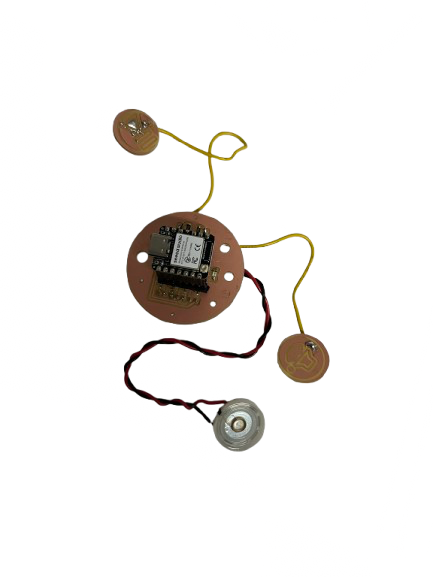
This week I added an audio output path to my custom XIAO ESP32-S3 board: a tiny class-D amplifier driving an 8 Ω speaker. The focus was on hardware design—schematic edits, routing, power integrity, and fabrication—so I can program it next.

Add an output device to a microcontroller board you designed, and program it to do something.
I implemented the hardware path first (MCU → amplifier → speaker). Firmware comes next.
I reused the circular ESP32-S3 board from Week 6. It already had: stable power, XIAO footprint, and generous routing space.
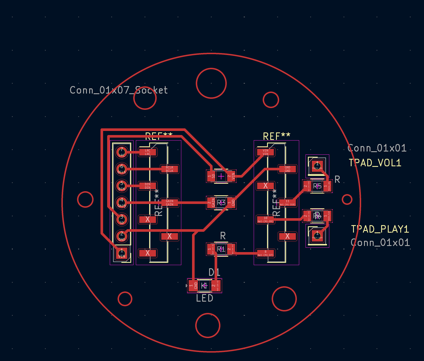
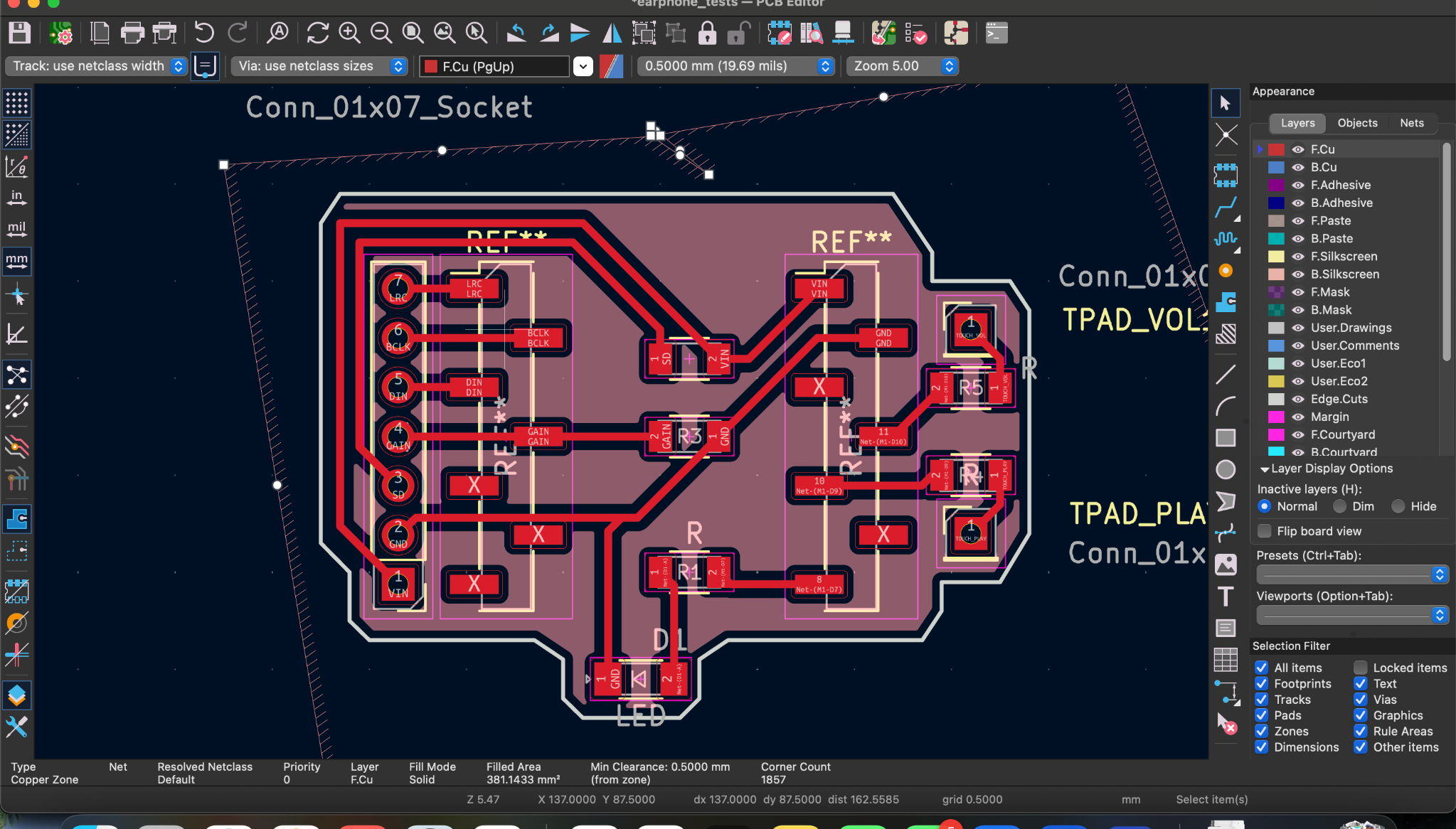
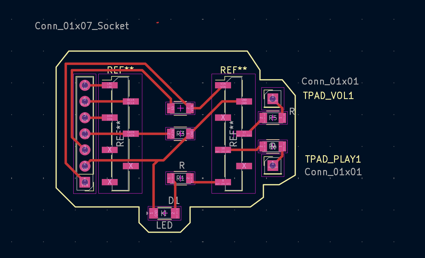

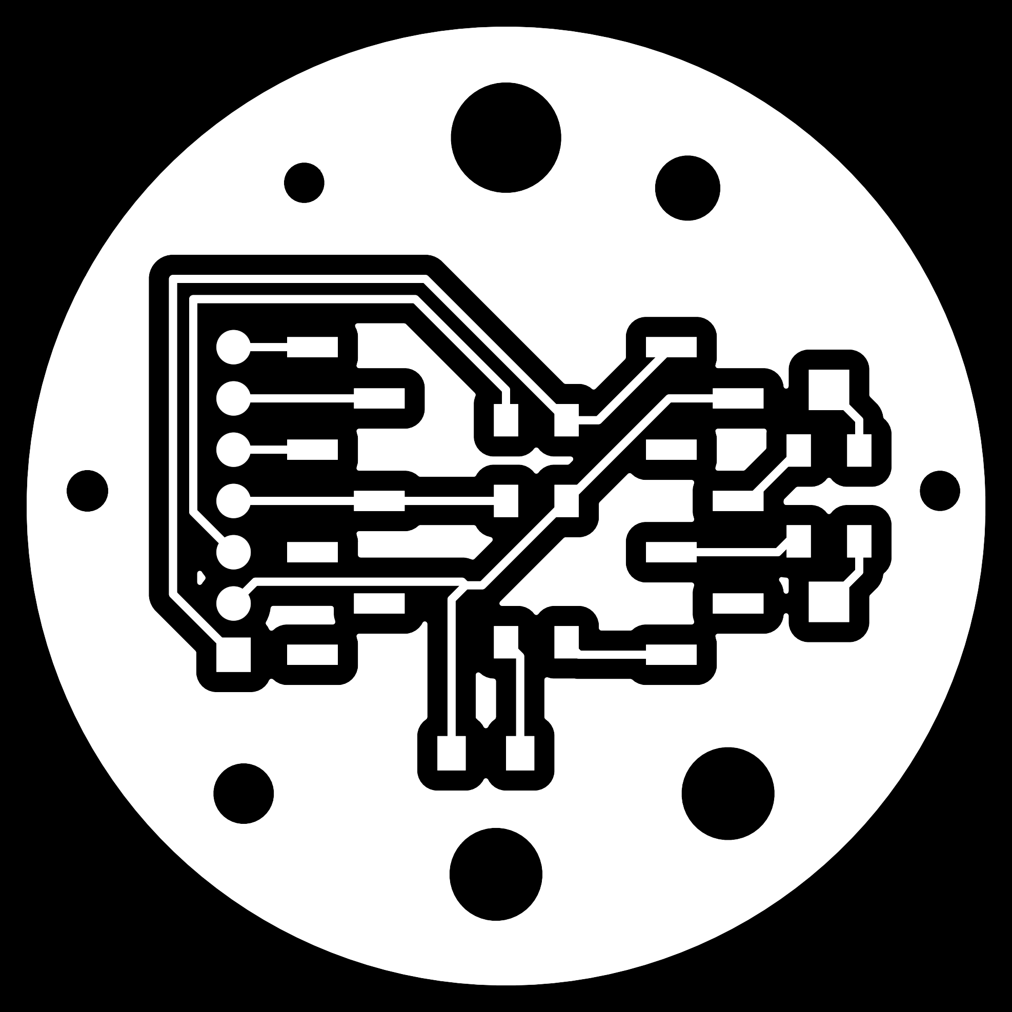
The class-D amplifier outputs a differential pair. I routed SPK+ and SPK− to large through-hole pads and left room for strain-relief heatshrink.

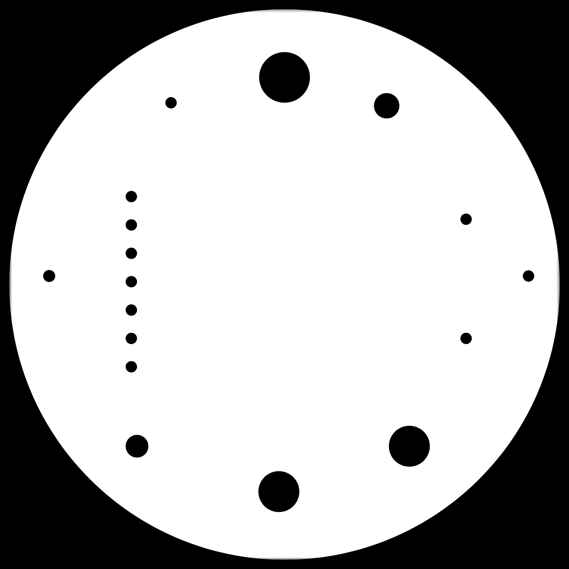
These are the fabrication PNGs I exported at high DPI for Mods:
The final board was exported as Gerbers and drills for manufacturing.
To satisfy the individual assignment requirement, I programmed the board and verified that the output device (speaker) produces sound. The ESP32-S3 drives the audio path while simultaneously updating the OLED display, confirming that the system is running user code and actively controlling outputs.
In this first test, the firmware initializes the OLED over I2C and plays audio through the amplifier and speaker while the board is powered over USB.
#include <Wire.h>
#include <Adafruit_GFX.h>
#include <Adafruit_SSD1306.h>

#define SCREEN_WIDTH 128
#define SCREEN_HEIGHT 64

#define I2C_SDA 2
#define I2C_SCL 3

Adafruit_SSD1306 display(SCREEN_WIDTH, SCREEN_HEIGHT, &Wire, -1);

void setup() {
  Serial.begin(115200);
  delay(500);

  Wire.begin(I2C_SDA, I2C_SCL);

  if (!display.begin(SSD1306_SWITCHCAPVCC, 0x3C)) {
    Serial.println("SSD1306 allocation failed");
    while (1);
  }

  display.clearDisplay();
  display.setTextSize(2);
  display.setTextColor(SSD1306_WHITE);
  display.setCursor(0, 0);
  display.println("Hello!");
  display.setTextSize(1);
  display.println("OLED is alive :)");
  display.display();

  delay(2000);

  for (int i = 0; i < SCREEN_WIDTH; i++) {
    display.clearDisplay();
    display.fillCircle(i, 32, 5, SSD1306_WHITE);
    display.display();
    delay(20);
  }
}

void loop() { }
GND.