Week 5
Electronics Design
10/01/2025-10/08/2025
Group Assignment
Here's the link to our group assignment: group assignment
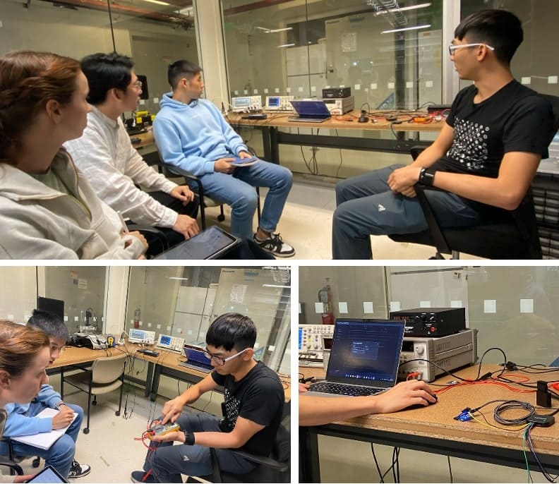
Alan and Nik walked us through how to use the multimeter, oscilloscope, and logic analyzer to help with debugging the boards.
Finding the parts I want to use
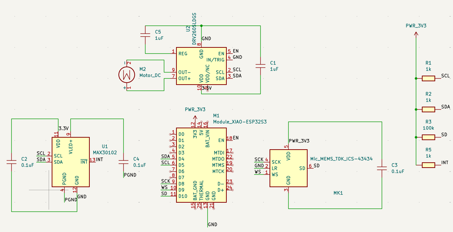
Since this week is highly correlated to my final project, I want to focus on using this week to start designing the board for my wearable device. In particular, I am looking at
- MAX30102 for heart rate tracking
- ESP32S3 as microcontroller
- ICS-43434 for audio input
- DRV2605 for haptics
I found the kicad library for ESP32 boards at
First Try
While starting to design the schematics, I quickly encountered several problems that I did not understand.
- I don't know where to add the resistors
- I don't know where to add the capacitors
- I don't know which pin should be connected with which
I searched all over the internet for electronics circuit design guide but wasn't able to find any guide on how to connect various components.
Fortunately, I found this example diagram, which helped me get started.
However, I was still confused on why there are a series of resistors on the left. I added it to my schematic anyways without knowing why.
Upon revisiting, I learned that these are pull up resistors to ensure that the I2C bus defaults to high voltage when no peripheral is pulling it down.
Reading the datasheet
Thanks to the help of the TAs, I started to understand the pinout diagram of my various components.
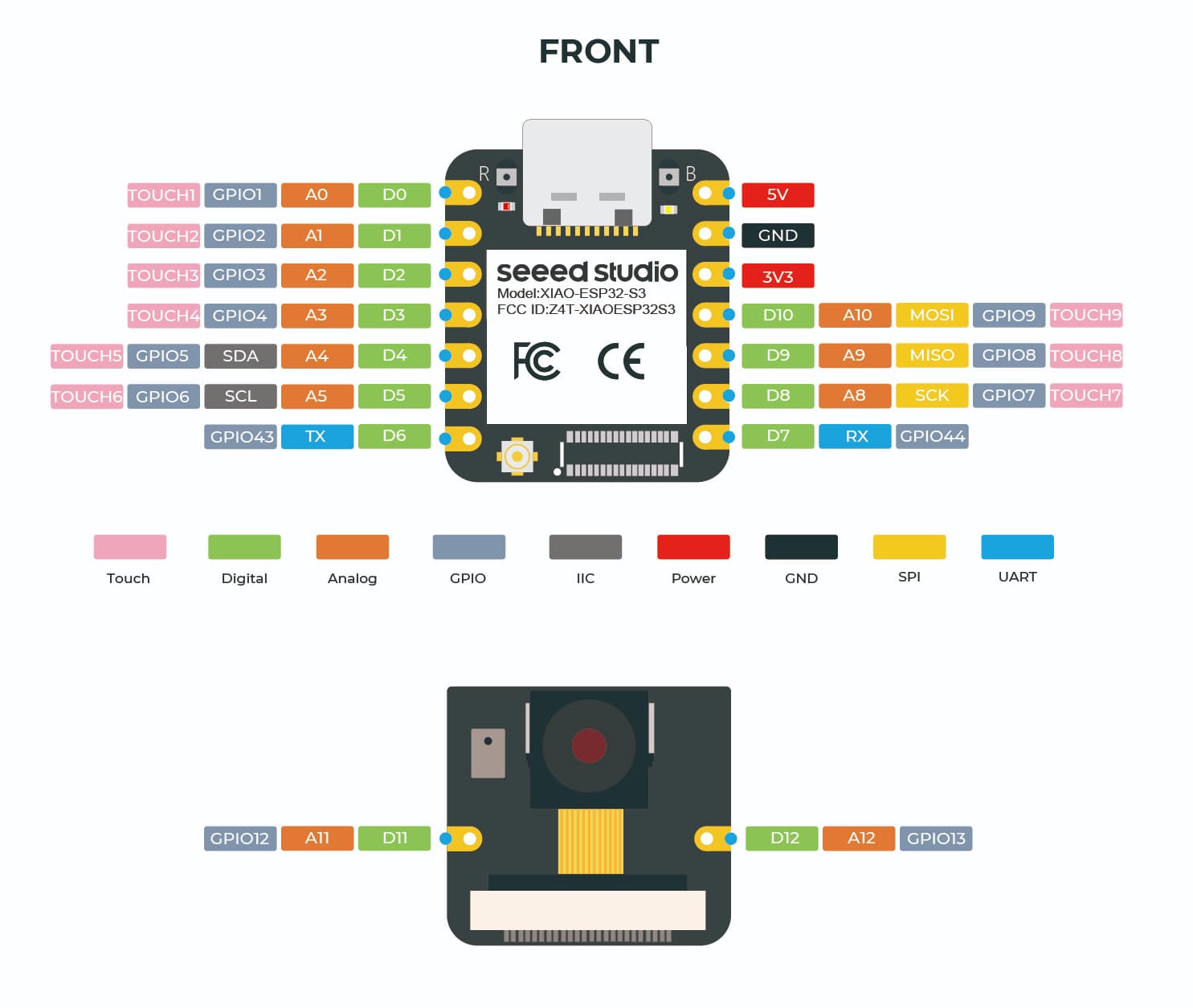
Now, I understand that I can connect SDA and SCL to D4 and D5 respectively. I also learned that I can connect the SCK from my mic to the ESP32S3 at D8.
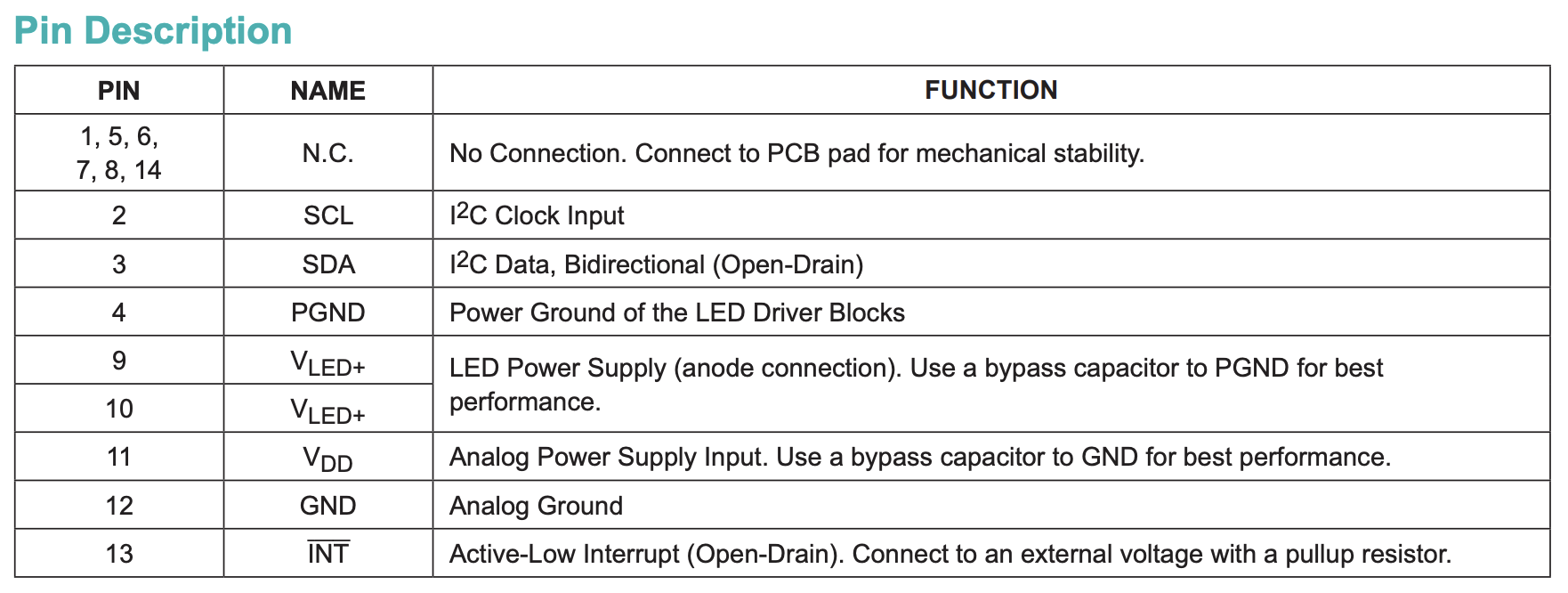
Looking into the datasheets of specific components, I found more details on how to setup my circuit. For example, looking at the pin description for MAX30102, I understood that I need to setup a bypass capacitor for VLED+ and INT to an external voltage with a pullup resistor.
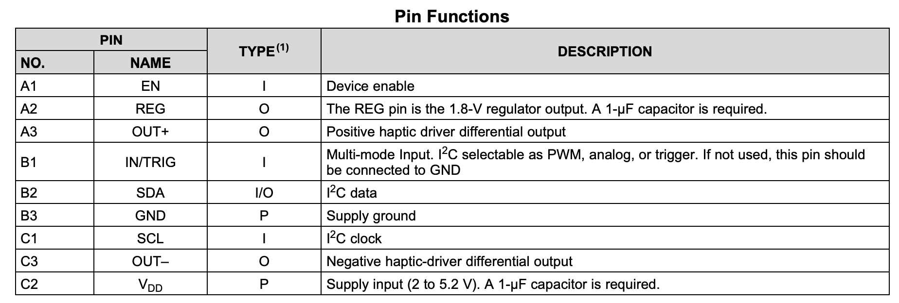
Another example is the DRV2605 haptics driver. The pin function table told me to add a 1uF capacitor to the VDD pin, as well as using the REG pin for a 1.8-V regulator output with 1uF capacitor.
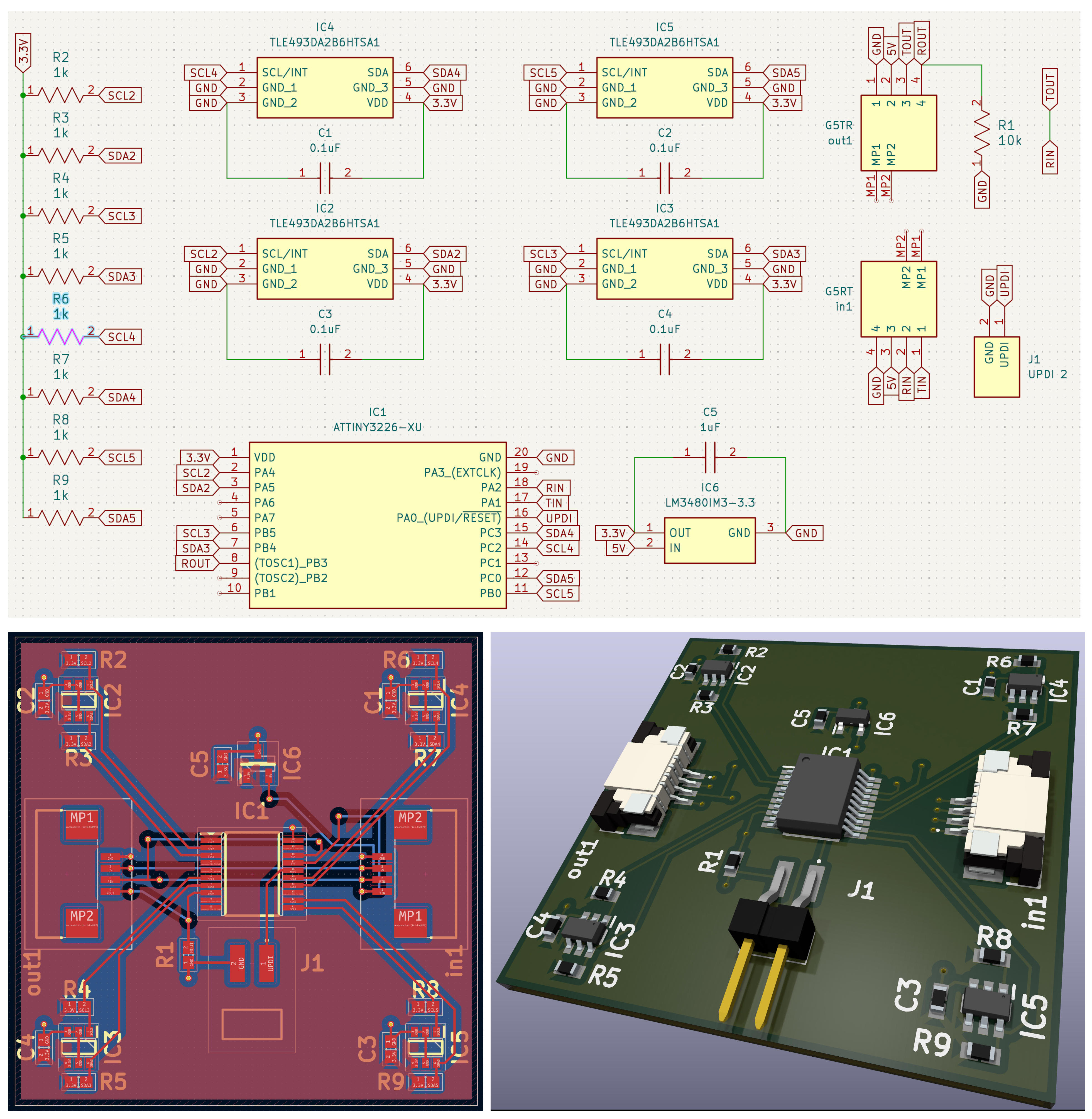
With all of these information, I am now more confident in designing my circuit in KiCad schematics. With many components added, I found that connecting all of the components with wire would make the diagram very messy, so I started working with using net labels to make the schematics cleaner.
PCB Layout
With the schematics designed, it is time to move on to PCB layouts now. I first set the constraints for
- Minimum clearance: 0.4mm
- Minimum track width: 0.4mm
Similar to the schematics, there are so many things to be connected and this time, I cannot use net labels to bail myself out. I had to move many components around and test the best location that would allow easier connections. I tried to do this by placing the components closer to the pin location, and the bypass capacitor and pullup resistor close by too.
The first thing I noticed was that there is no footprint for my motor, so I used a PinHeader_01x02_P2.54mm_Vertical_THT_D1mm instead to represent my motor.
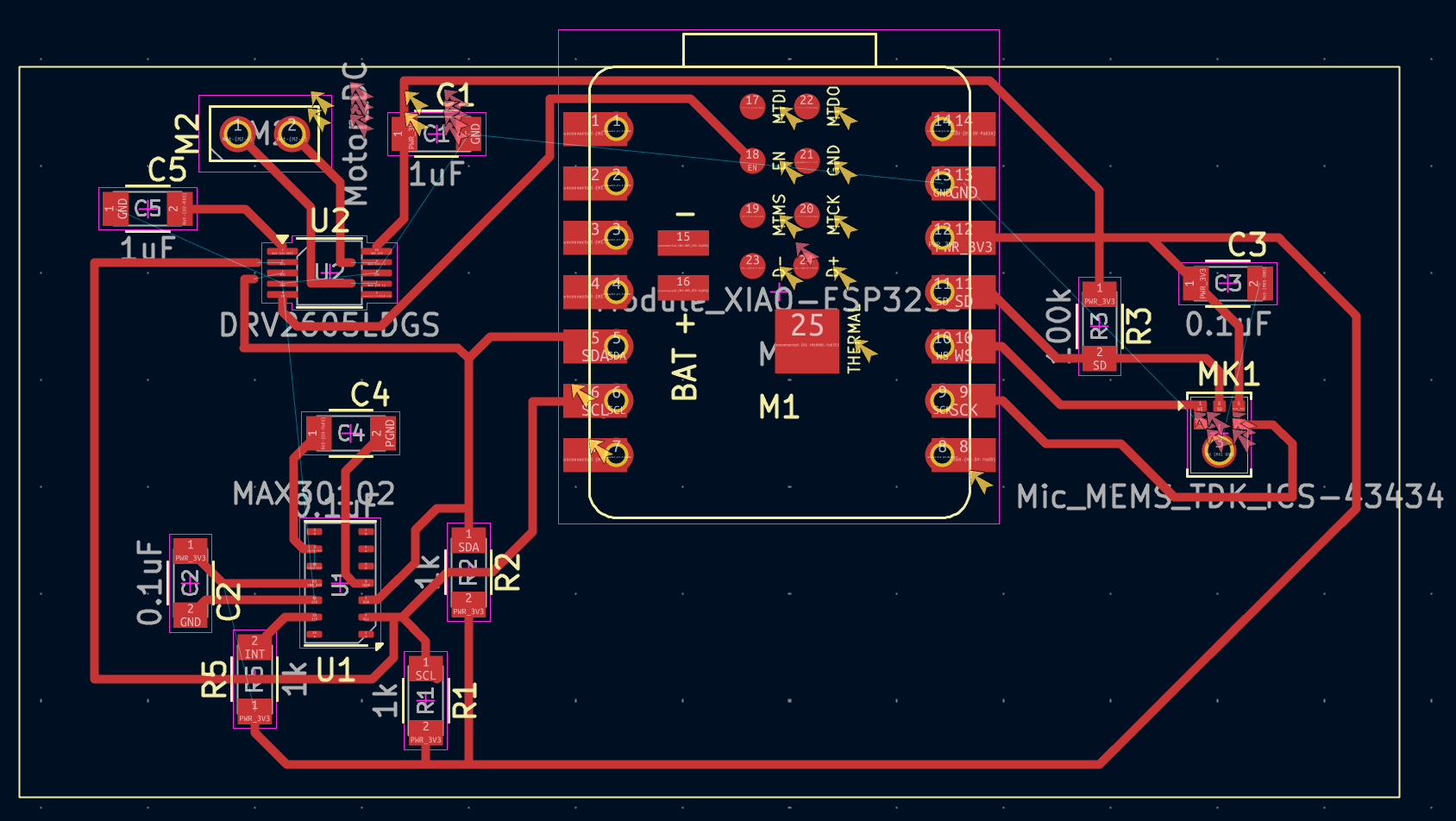
After eventually setting up all of traces, I ran the Design Rule Check. Bam! 28 errors. Looking through the errors, it mostly has to do with the component footprint has pins super close together, with values such as 0.2mm, 0.3mm, and 0.346mm. These are closer than the minimum clearance of 0.4mm suggested by Quentin during the recitation.
So it seems like the next step would be to either edit the footprint so they satisfy the constraints or I can remove the constraints. I am not sure if editing the footprint layout would conflict with the real part that I will be using from the inventory. I also need to add the fill and connect the GND pins to the fill.
After consulting with Anthony, I reduced the clearance to 0.3mm while also editing the footprint to have the pins farther apart from each other, which was preventing the traces from connecting before. I added a circular edge and added a filled GND zone.
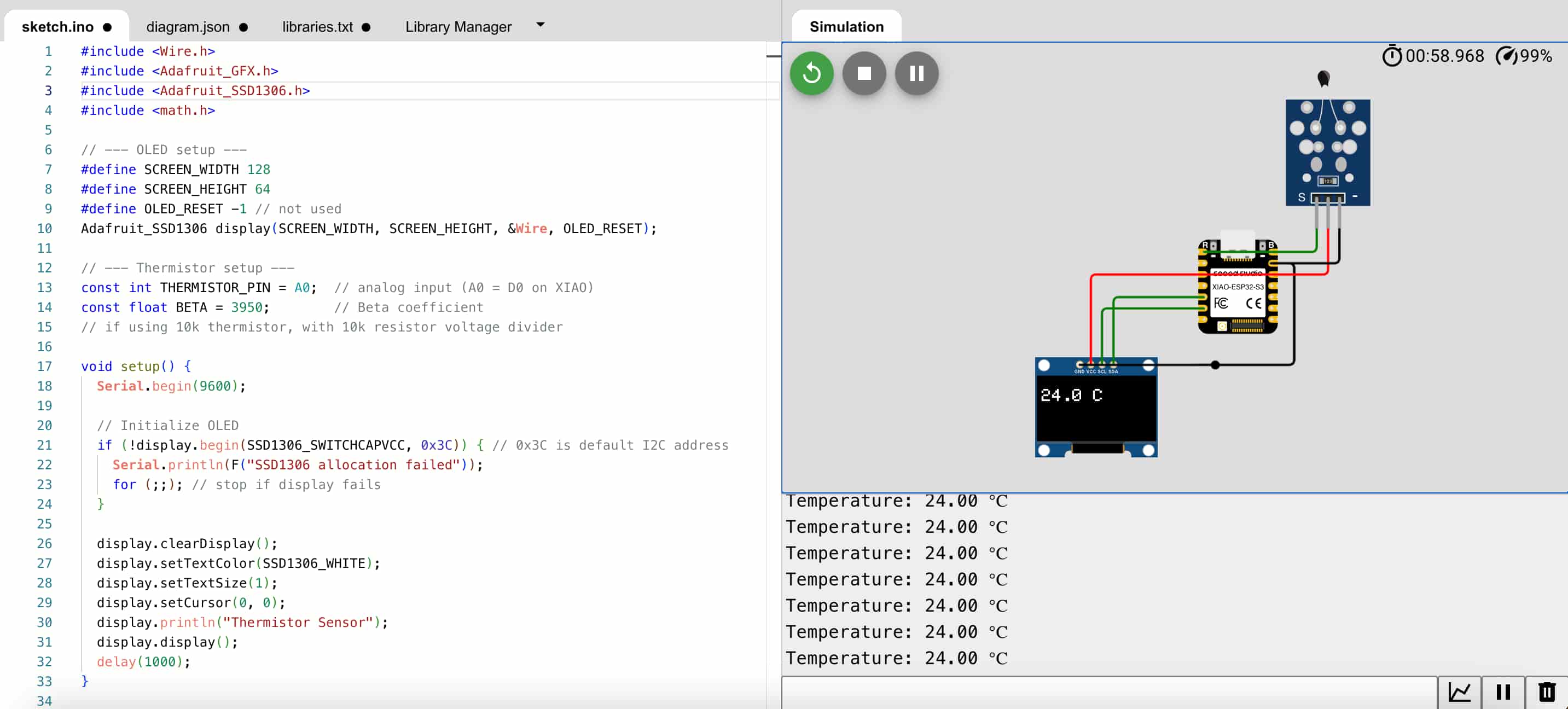
Simulation
Thanks for dropping the part to simulating my circuit! I would have no idea on how to even begin.
Now, I aim to simulate a simple circuit using WokWi using the XIAO ESP32-S3 microcontroller that I will be using.
I came back after finishing week 6 to complete the simulation. I used the final simple circuit I designed using the NTC Thermoresistor and the OLED Screen. I successfully read the temperature from the sensor and displayed the temperature on the screen.
Resources and Acknowledgements
Tools used:
- KiCad
- WokWi
Thanks to Alan, Quentin, and Anthony for answering my questions.
Design Files
You can download the KiCad design files here
You can download the WokWi simulation files herehere