Week 6
Electronics Production
10/09/2025-10/16/2025
Group Assignment
Here's the link to our group assignment: group assignment
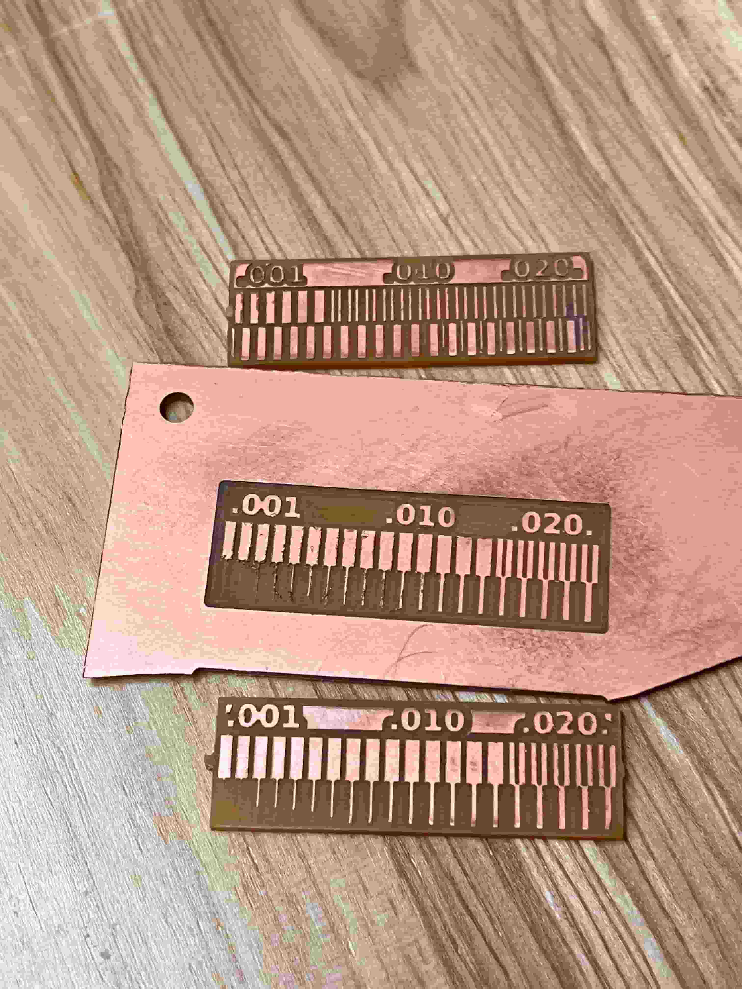
For the group assignment, we first characterized the design rules for our in-house PCB production process. Then, we worked on sending a PCB design to the board house.
Electronics Production
I first started to work on milling the board I designed last week. However, when I started to print my board I found that the probing is actually going outside the board I chose. I wanted to design a small circular board for my wearable product, so the dimension should fit on the board I chose to mill. I went back to my design and found the problem. I wanted a circle edge with diameter of 40mm, but instead I didn't notice the dimension is 40mm radius, so I got a circle with 80mm in diameter.
So I went back to redo my design so everything would fit on a smaller board.
Here's the new design and the board it cut out.
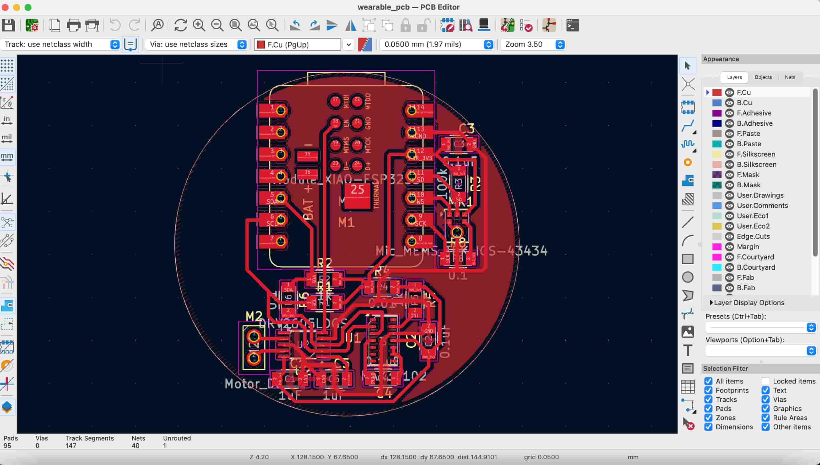
I noticed that many of the details are not done right due to the tight arrangements I had. So I went ahead and removed the MAX30102 and DRV2605 components since those are still being shipped anyways. I tried to add more space and clearance to my design and milled another board.
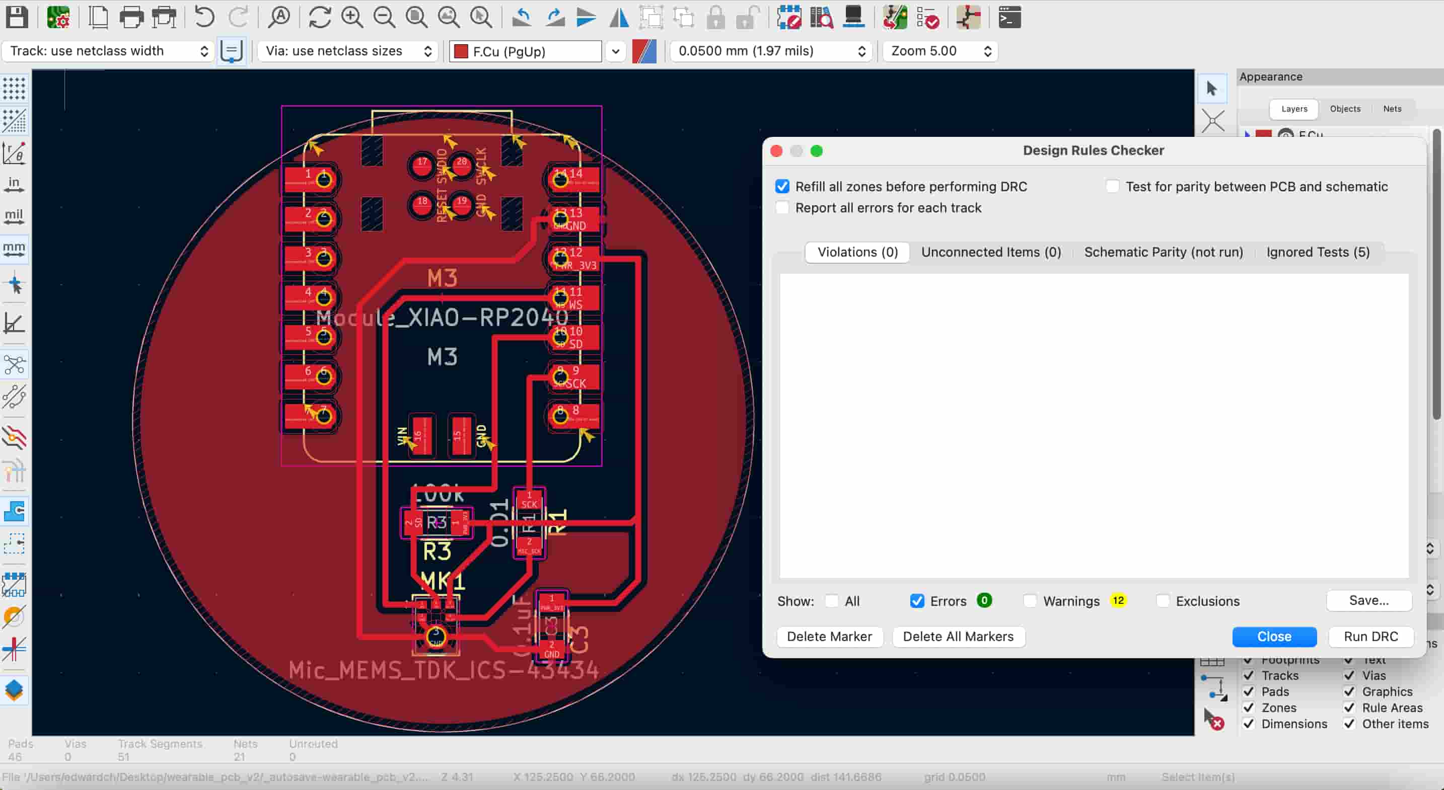
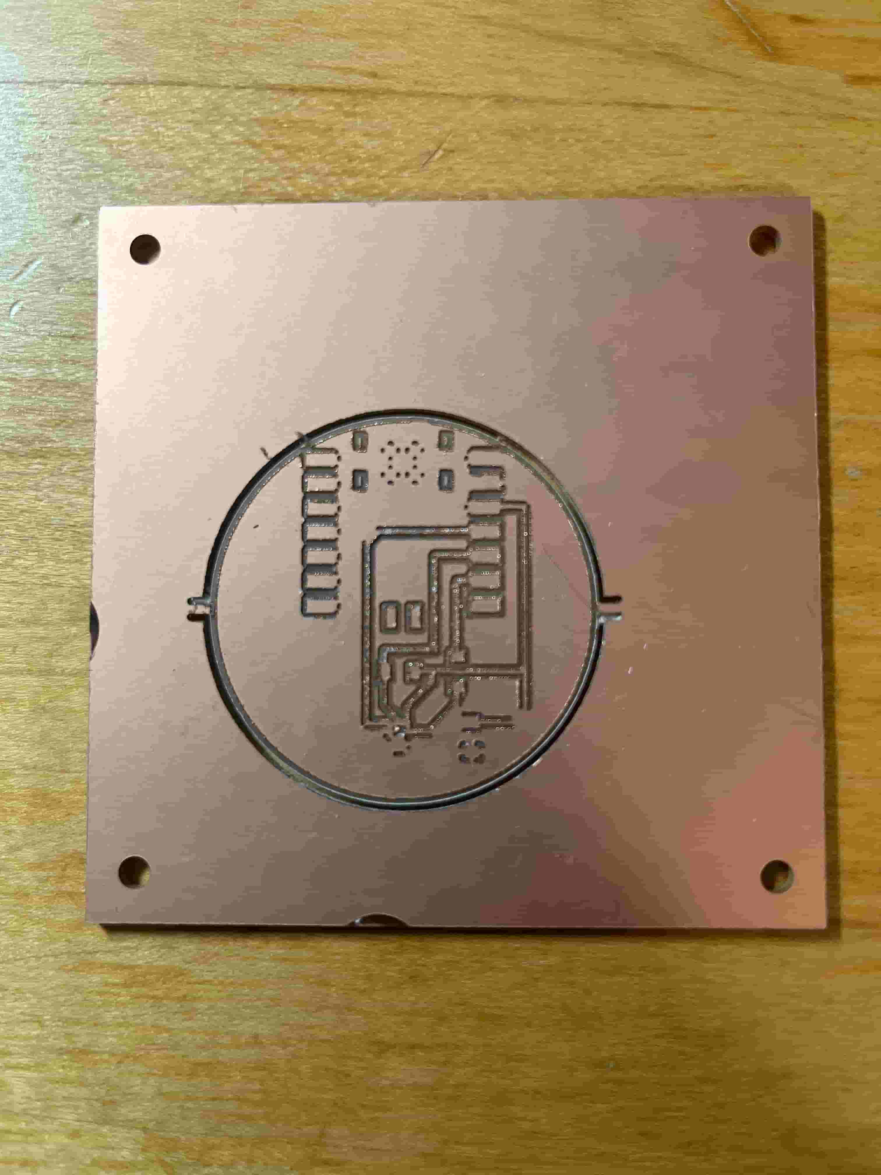
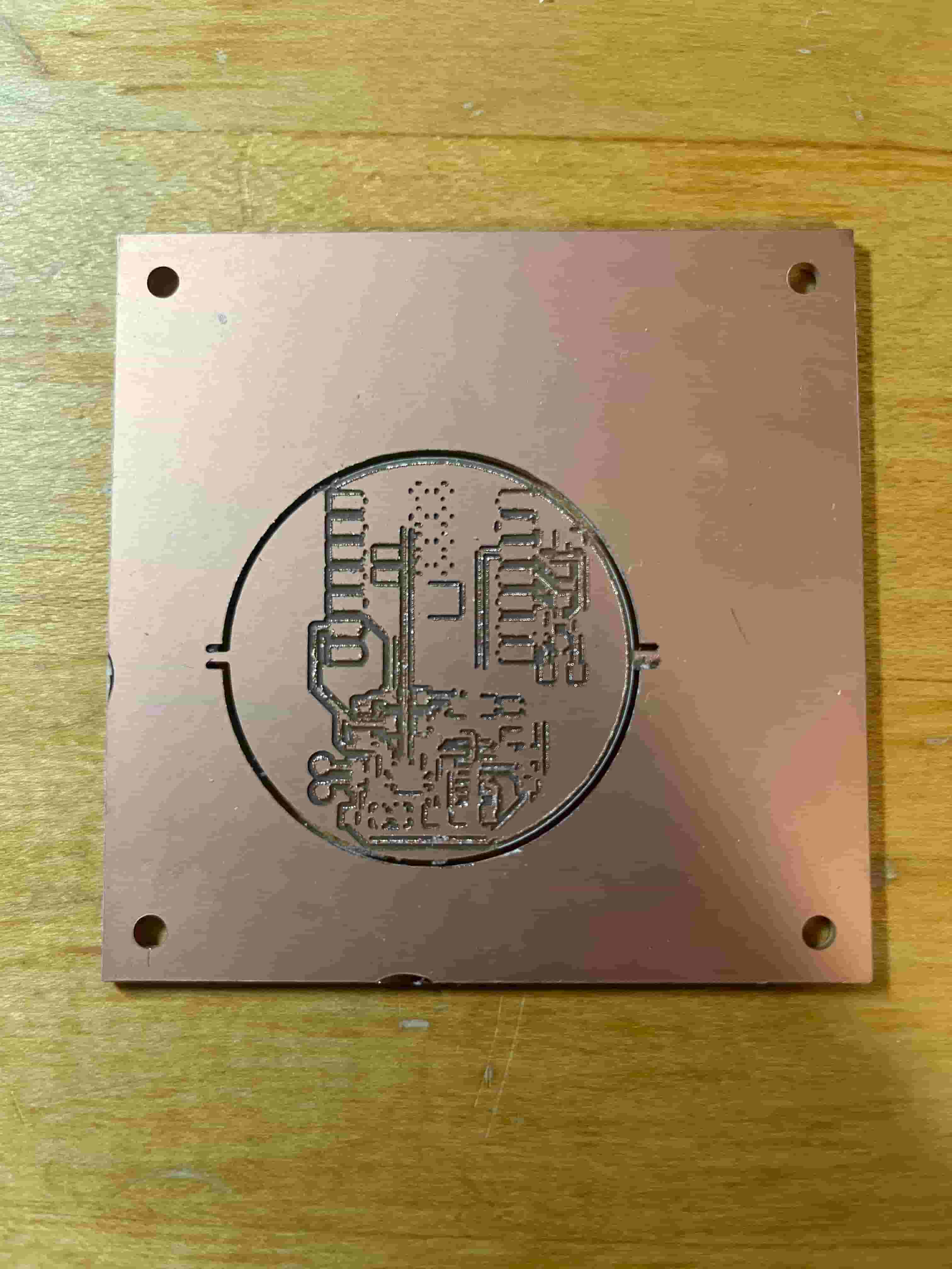
Again, there are some traces that are not cut out, and the part where I am placing my ICS-43434 mic is simply not cut properly. I believe this error is happening because the ICS-43434 is very small and the clearance between each pin is smaller than the required 0.4mm. In fact, during the Design Rule Check, I reduced the minimum clearance from 0.4mm to 0.3mm to remove some of the errors.
In order to produce a board with finer details, I need to turn towards laser cutter, which I will be learning from Quentin on how to use. This will also encourage me to try out a new workflow.
New Design
In the meantime, I want to build something simpler that would satisfy the requirements for this week. I then wanted to work with larger components that would be easier to mill and install. I landed on the following components:
I created a new design to fit all of these components.
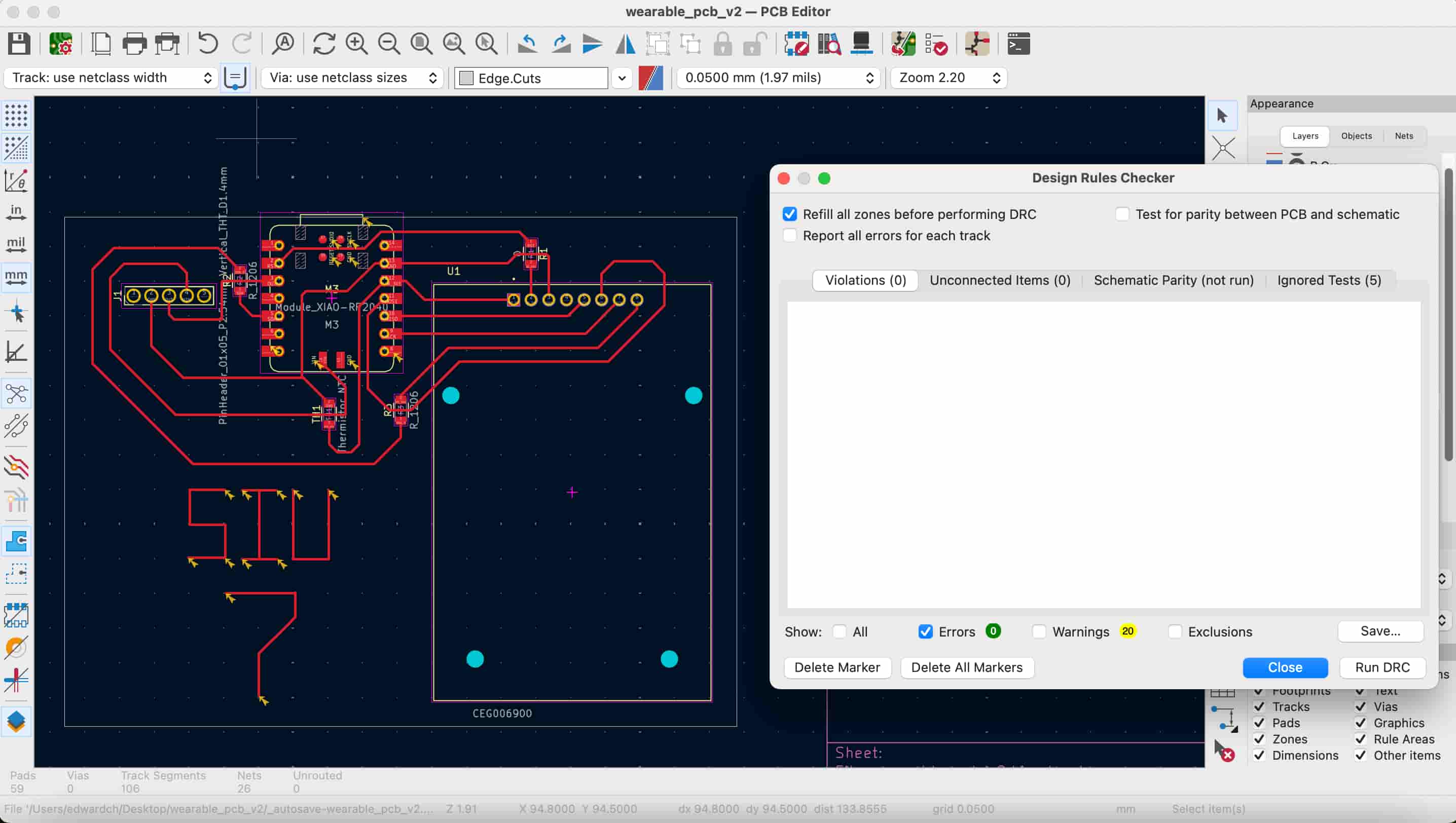
However, I encountered another problem when sending my design to Carvera. I noticed that some of the traces did not appear in the GCode file.
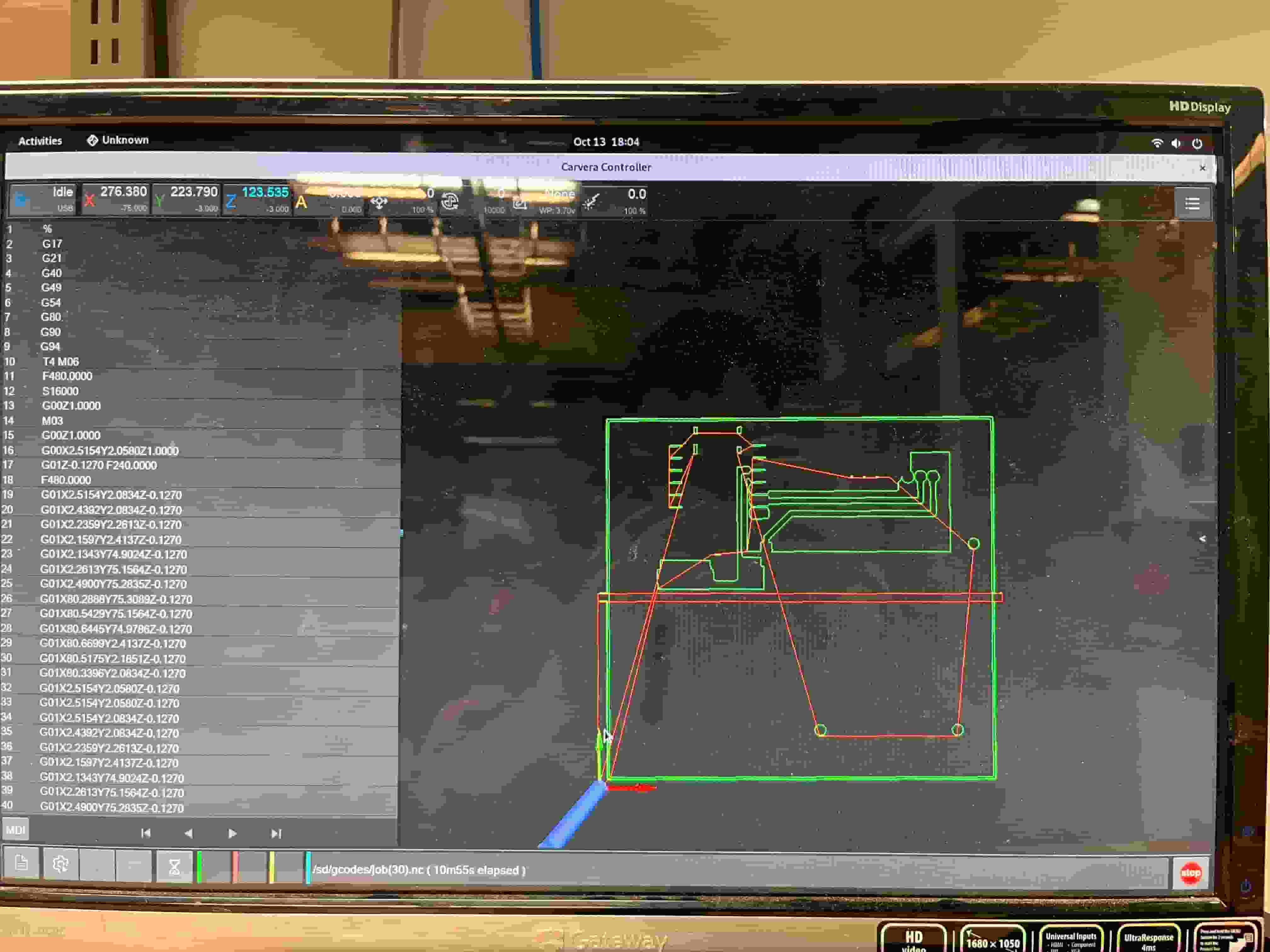
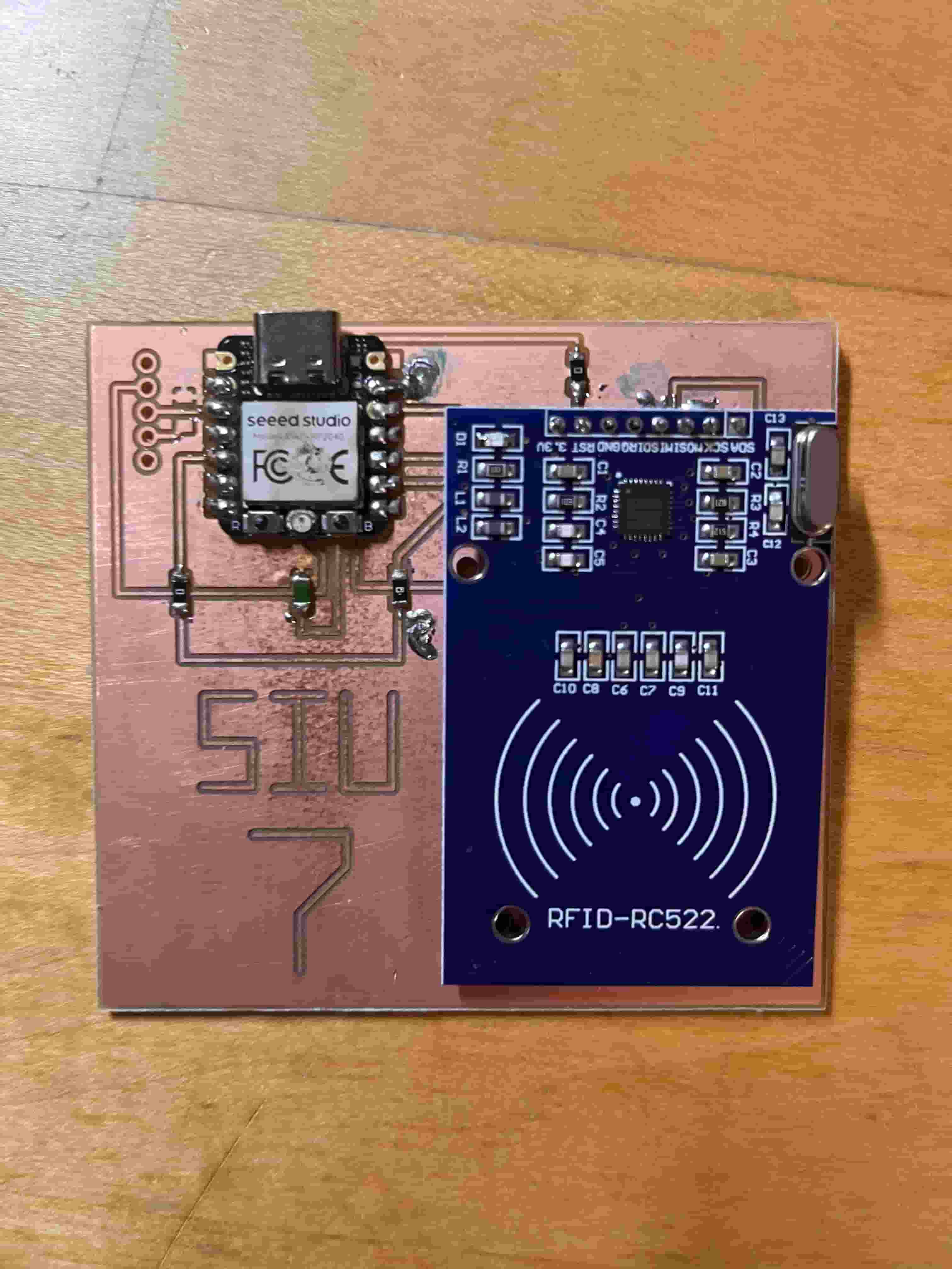
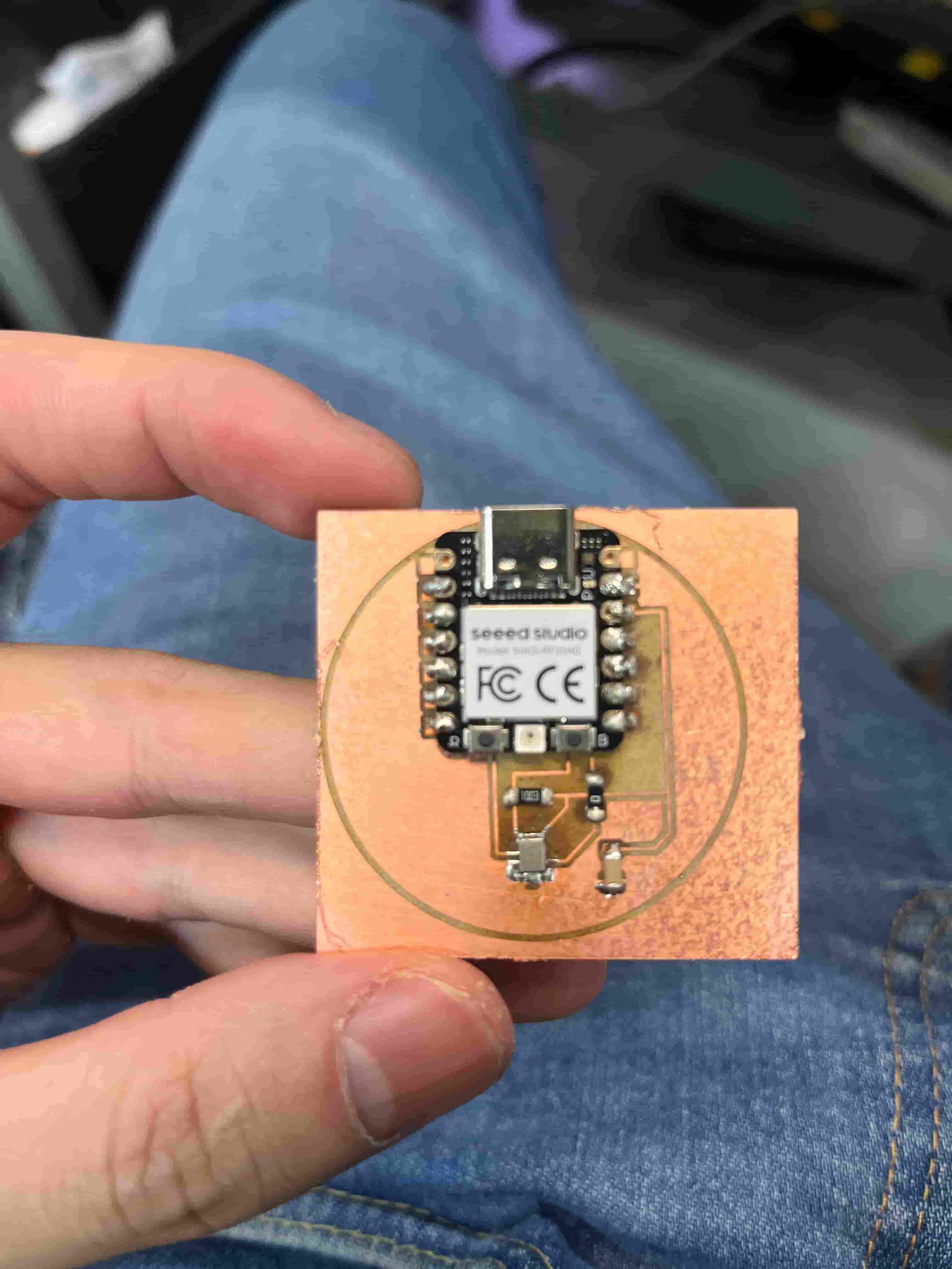
I improved my design by leaving wider clearance between traces. And I got a board that I can work with. I did notice that I used one of the VIN pins, which is at the bottom of the XIAO RP-2040 microcontroller, so Huanyu helped me with applying the solder paste to connect.
Laser Cutting
Quentin showed Sun and I how to use the xTool F1 Ultra laser cutter to create our own PCB board. I learned how to use laser cutter to create my PCB board. Thanks to Sun for staying with me to configure the settings.
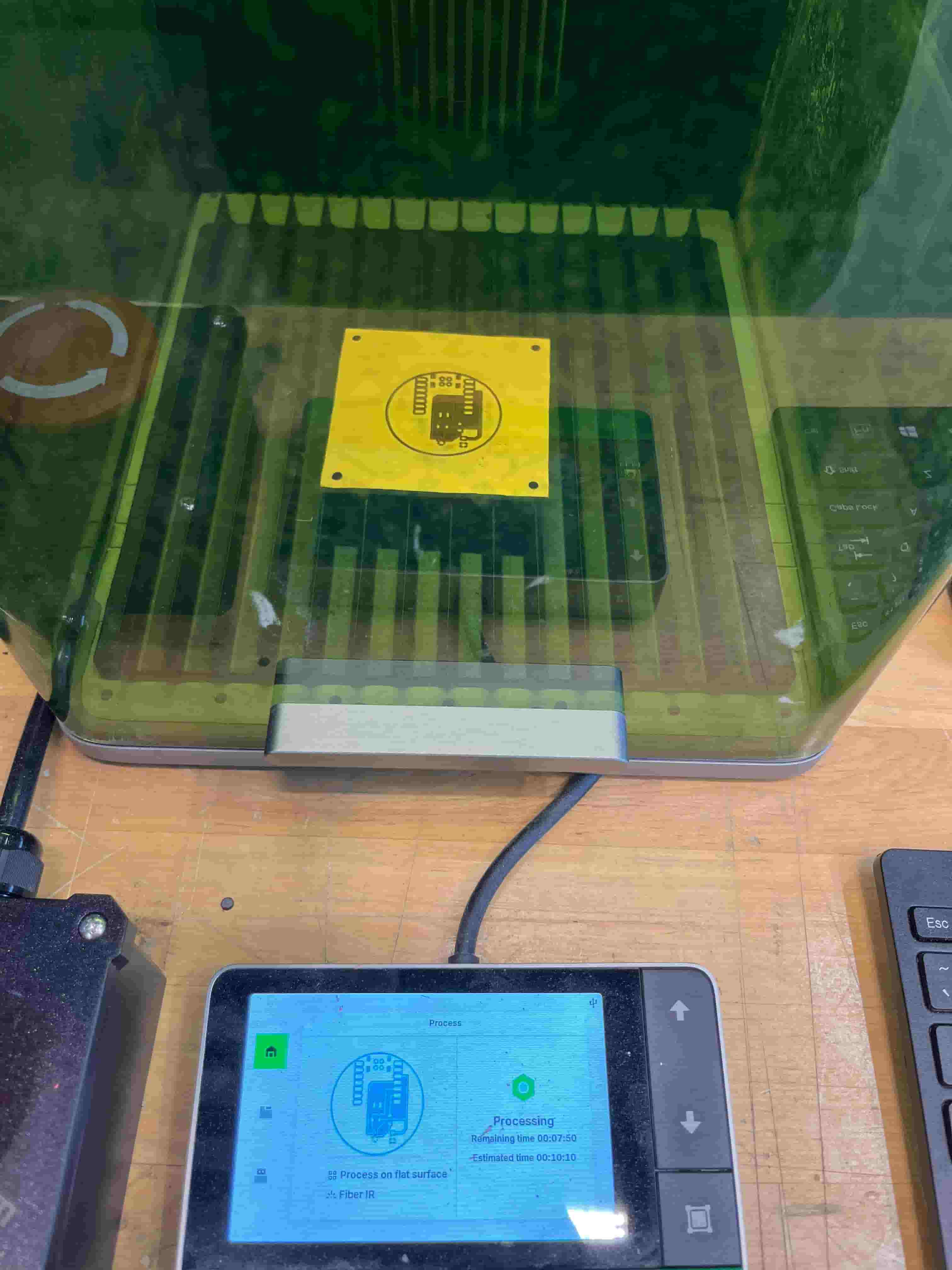
Here's the setting I used to create my board, and it is stored on the machine under the name PCB:
- Laser Type: Fiber IR
- Power: 100%
- Speed: 750mm/s
I finally printed the board that I designed and can start soldering components onto it. I held my breadth and quickly brought the board to rinse with soap, as Quentin said the cut might've generated toxic materials. Then, I used the sandpaper to refine the board.
Since the ICS-43434 component is tiny, I used the soldering paste and the heating gun to attach it to the board. After soldering the XIAO-RP2040 as well as the resistors and capacitors, I ran continuity test and saw that all the traces are connected properly. It is hard to know whether the mic is properly attached since all the pins are hidden at the bottom.
How to Fail Almost Anything
After long hours of testing and debugging the some sample code for both of my boards, I realized that I made a few mistakes in my circuit design. First, I cannot connect the LR pin of the ICS-43434 to GND. The sample shown in the datasheet used two ICS-43434 so one of the LR went to ground. In my case, I need to connect it to one of the pins to indicate pins to show the left/right channel select. For the thermoresistor, I directly connected the 3.3V to one end and the other end to GND. Instead, I should have it in a resistor series, with another 10k resistor. The RFID chip reader is also not reading the card value, and I have no idea why.
After learning these mistakes I made, I had no time left and have to resort to the simplest design I can think of. Let's just throw together a thermoresistor and a microcontroller. But I think the process of working on two boards and changing my design constantly actually made me a lot more confident in looking through the datasheets and working with KiCad.
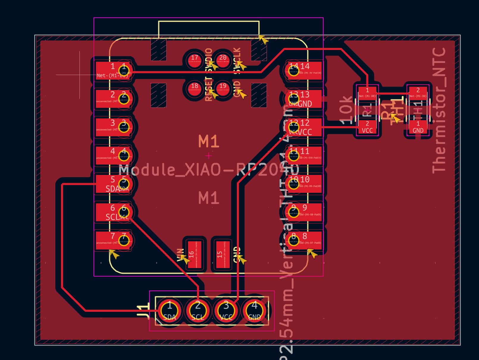
This also didn't work unfortunately because I didn’t realize you need a 100 kΩ resistor in series with the thermistor to form a voltage divider for reading the temperature as a voltage. I believe I also needed to connect the thermistor to a GPIO pin for the microcontroller to read the temperature through the voltage drop.
I did test more than one process for producing a board and I believe laser cutting a board will be crucial for making the board for my final project.
Resources and Acknowledgements
Tools used:
- Carvera Desktop CNC
- xTool F1 Ultra
- Gerber2img
- KiCad
- Arduino IDE
Thanks to Quentin for teaching the skills needed for this week. Thanks to my friends for helping with my questions.
Design Files
You can download the KiCad files for RFID board here
You can download the KiCad files for laser-cut board here
You can download the KiCad files for thermistor board here