# Week 5
## Electronics Design
### Group Assignment
Gert explained to us how it can be helpful to think of electricity as water flowing through a tube. While this is not what is actually happening, it is helpful to understand voltage and amperage, and how resistors and capacitors work.
Writing about this helped me really understand or at least remember the difference between Voltage and Amperage.
| 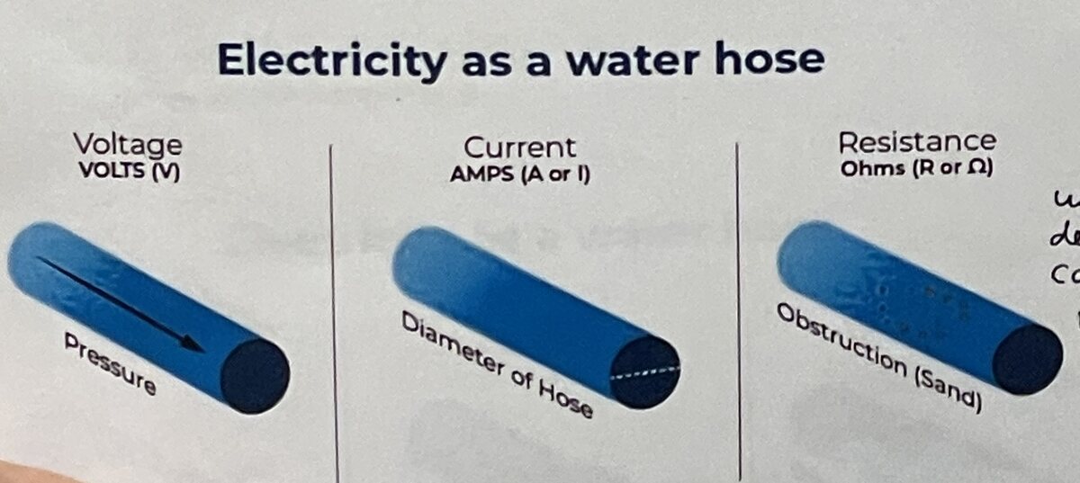 |
|:---------:|
| *Electricity as a water hose* |
Here it is in my rough understanding:
- Electricity is electrons wanting to go from one point to another (they actually travel backwards from negative to positive).
- Voltage is the difference between two points, in very rough terms *how badly* the electrons want to go from one point to another. In the metaphore it is the pressure of the hose.
- Amperage is the *how many* electrons want to go from one point to another. In the metaphore it is the diameter of the hose.
- Resistance is *how difficult* it is for electricity to go between two points. Electrically conductive materials like copper or steel have a low resistance, something like clay has a high resistance (there is a lot preventing the electrons from going through).
Capacitors can be thought of as water tanks in this analogy. This is why they help smooth out an intermittent current.
|  |
|:---------:|
| *Capacitor as water tank* |
> Use the test equipment in your lab to observe the operation
of an embedded microcontroller.
Gert showed us how to use an oscilloscope to see a binary signal output from a raspberry pi microcontroller's pin.
| 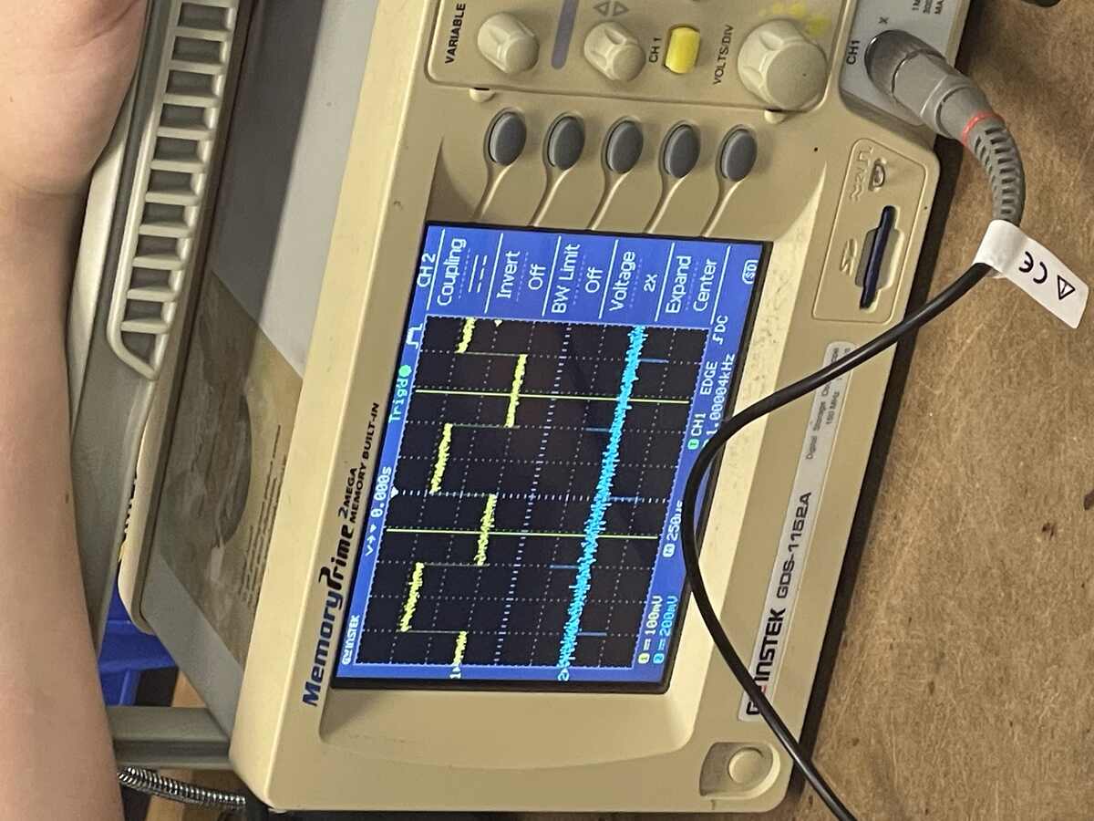 |
|:---------:|
| *The Oscilloscope measuring a binary signal (we see a square wave)* |
We also learned how to use a voltmeter. In particular, you can quickly debug connections by pressing the mode button and getting a sound signal that will create a beep whenever the two probes from the voltmeter are connected.
| 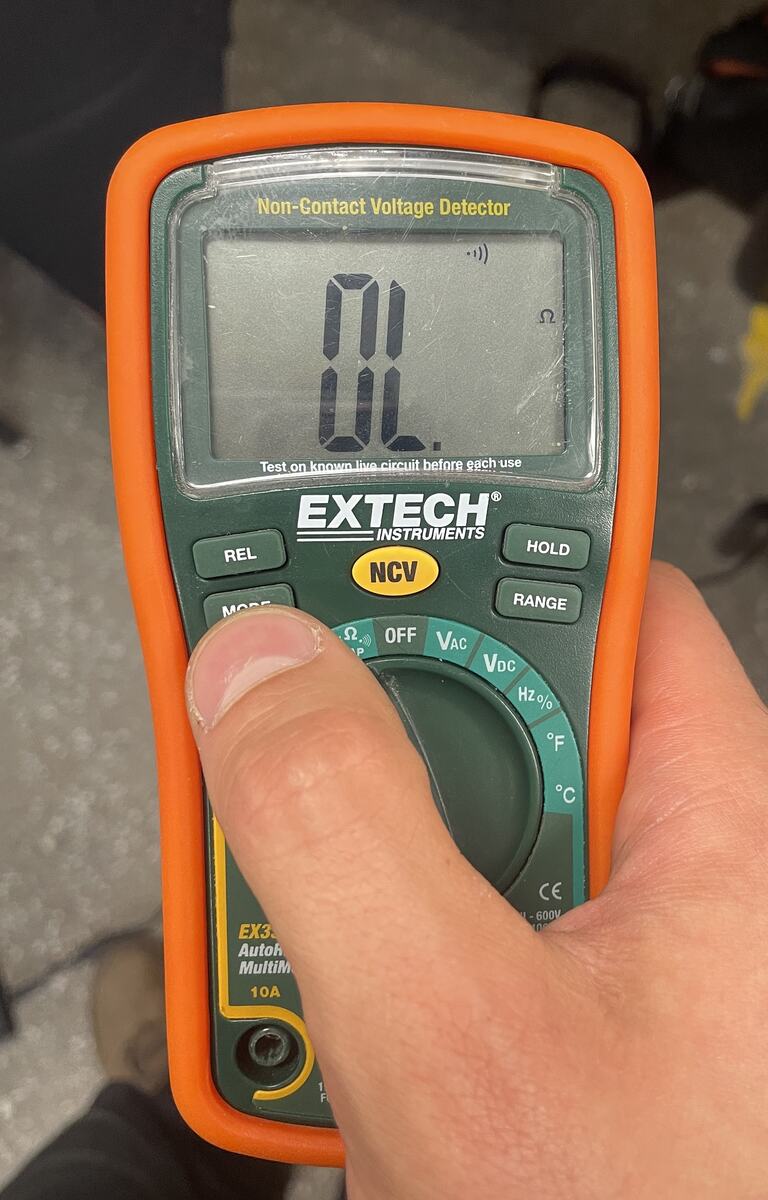 |
|:---------:|
| *The icon top right of the screen that looks like a WIFI signal will make a sound when 2 wires are connected* |
### Individual Assignment
> Simulate a circuit
> Use an EDA tool to design an embedded microcontroller system
using parts from the inventory, and check its design rules for fabrication
I will start with the RP2040 in the XIAO package, since it is the easiest to get started with, and I already made a board during the coding week that I can use as a starting point. The board was the [qpad-xiao by Quentin Bolsee](https://gitlab.cba.mit.edu/quentinbolsee/qpad-xiao).
| 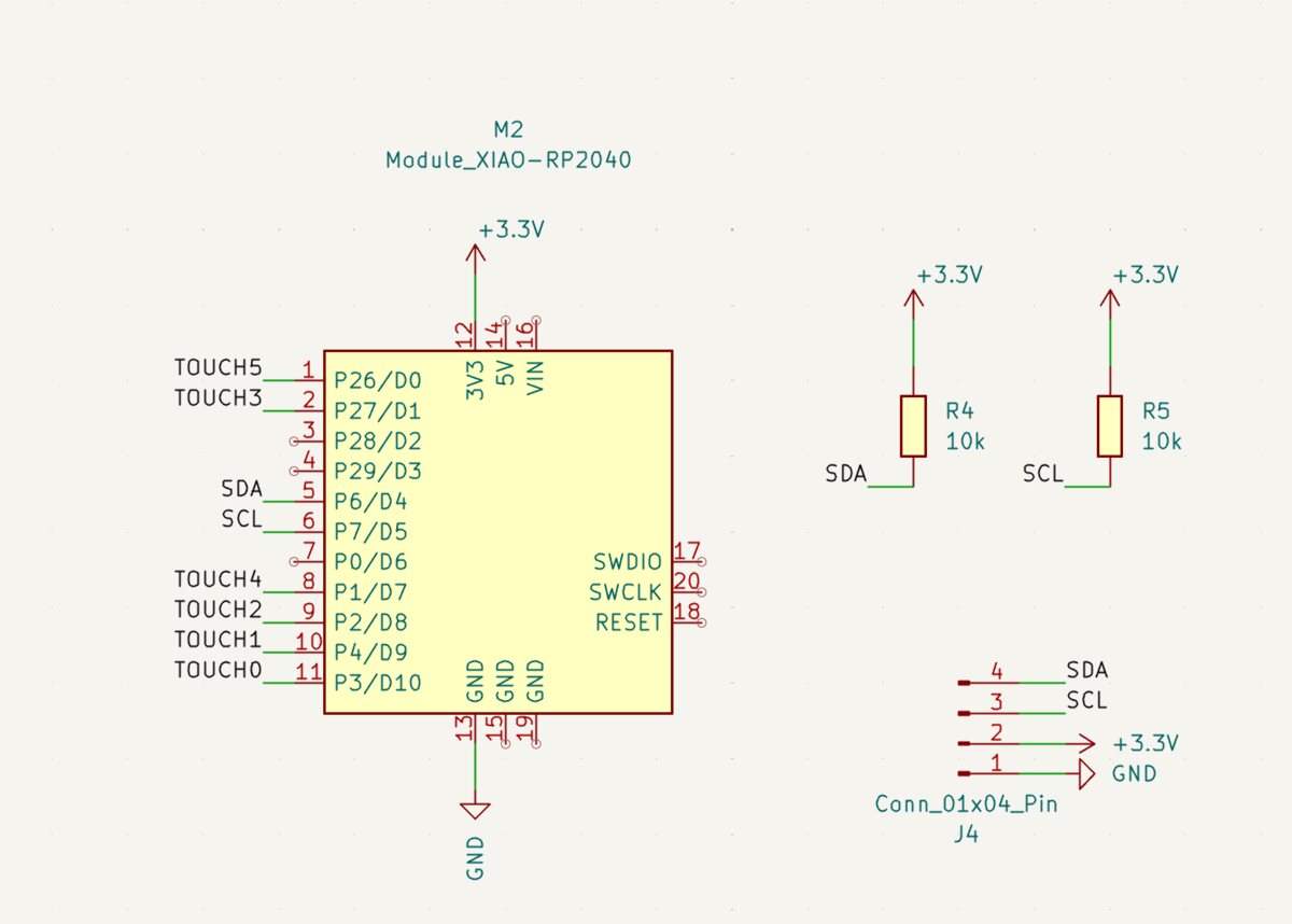 | 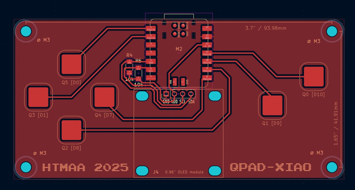 | 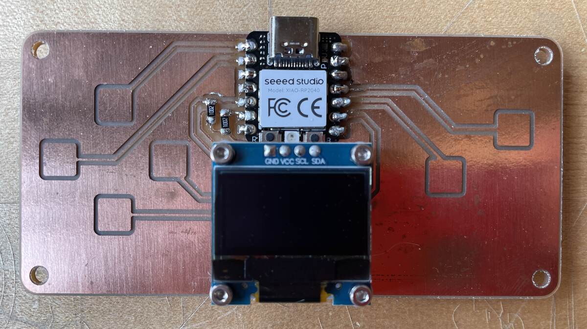 |
|:---------:|:---------:|:---------:|
| *Schematic of the Qpad RP2040 Xiao* | *Image of the Printed Circuit Board (PCB)* | *The stuffed board with components* |
#### Getting started with KiCad
I followed the [recitation by Quentin](https://vimeo.com/1124302535/cbe009f9f5?ts=0&share=copy&turnstile=0.BWKZ3gsyM3kB4n8Kd38cSxb6W4lpIOWnF4PNJYX6YpXBCSQb-k51jq0T2eG007S5ggk-lmgKWIeD9Dkdkl7VBugbJVS65JW1zK8aNL0FcWi5j_BtvvICB3624HQt5XMacMKeAJsi5vCpl1czWT0wXFtfmS6E8tZLooAWszUcW2l0dhv1u9ruX6RX9MsvrLhEMw9Y2WtHaKuj4hB5zNFqBDHH2jhNf1hUyOW2YwbNe7TWCh2K3LOQ-uijDRHwV4bDrNANZ7zNBtiCAf9bzzbHu7786cX1AY3oeUxECZpKY7p1PqfUdrrwhj3mwqplEp9_LpgKcmGGCB_1jPC4jh-NP6h3EHzSuw3qMM_dRd5xApyRh7QCVKKpjCseWLEqzC9WYzhc9_h8XnCxKhdZWAM8n-Q1FASgUuN4UNt0aaUmZ3Zal86-b3MttPP3kk4WZfhsVoVNyLIT9JNKWbRhIHCM8Igclwj9pbTHBbsHkY2OL7pmiir-iS3zSNGdIeS1oEzD2sA9qi8U3MRy6Crmimm-yna50TGORIM3feoiu5uNm9Rm0t2YA0KdwY2cHUePXhHmSSxaglIPm1wrVF1scWxODYQhG38LZHORhi8PsMJyzcTQ3NnP7WhyGgf0vzzsVoXUHtpBLKgx2X7w9xeM9UHhaJ_ujvYqFWdGr4-S6zhRDBcGL-nrIbHHxr5lN8LnwSu1MroDwSGh9orURYaDLK8JrZYcmDA2A1r1lwc3BpQsipIiOrSXE8kVfoFVAWZlpl_d4u5STggLN-Gogs2MmLZQl93w1Ap65d14VnLjxCCvSdpyHncZa4ZKcxOT48XLa_qBFQCJGpeoDn4UNKVG9A7vyPKhBrqOfuXn5vlDzSqm4sY.tWB1JXJ8aF8ppu-pMvO6xQ.f2ad3d6003030e99aa8e6ab0343d695cf0ebbfe7c0fcd48b9e60a64a311b790a) to get started with KiCad.
1. [Download KiCad](https://www.kicad.org/) (anything later than Version 8 is great)
2. Download the parts library from this [KiCad library git repository](https://gitlab.fabcloud.org/pub/libraries/electronics/kicad).
| 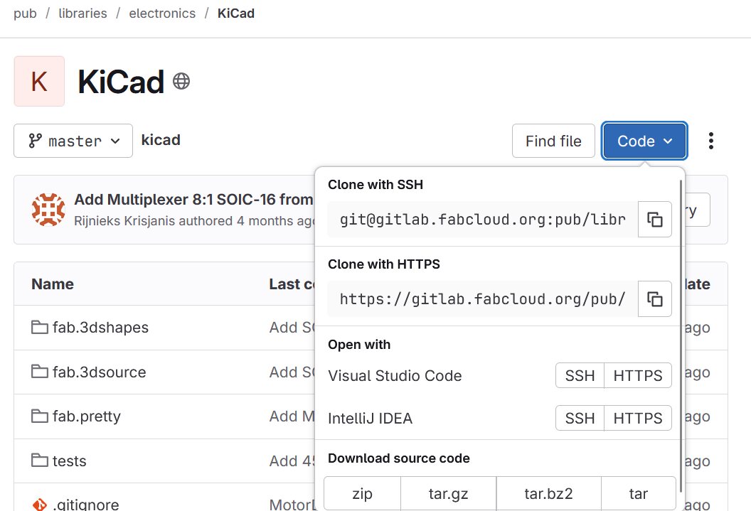 |
|:---------:|
| *Clone the KiCad Library from the Repo* |
Since it is a git repo, you can pull from it to get most up to date components!
- `fab.kicad_sim` is where the symbols live
- `fab.pretty` is where the footprints are
- The folder has a subfolder called `fab.3dshapes` which has all the 3d data
| 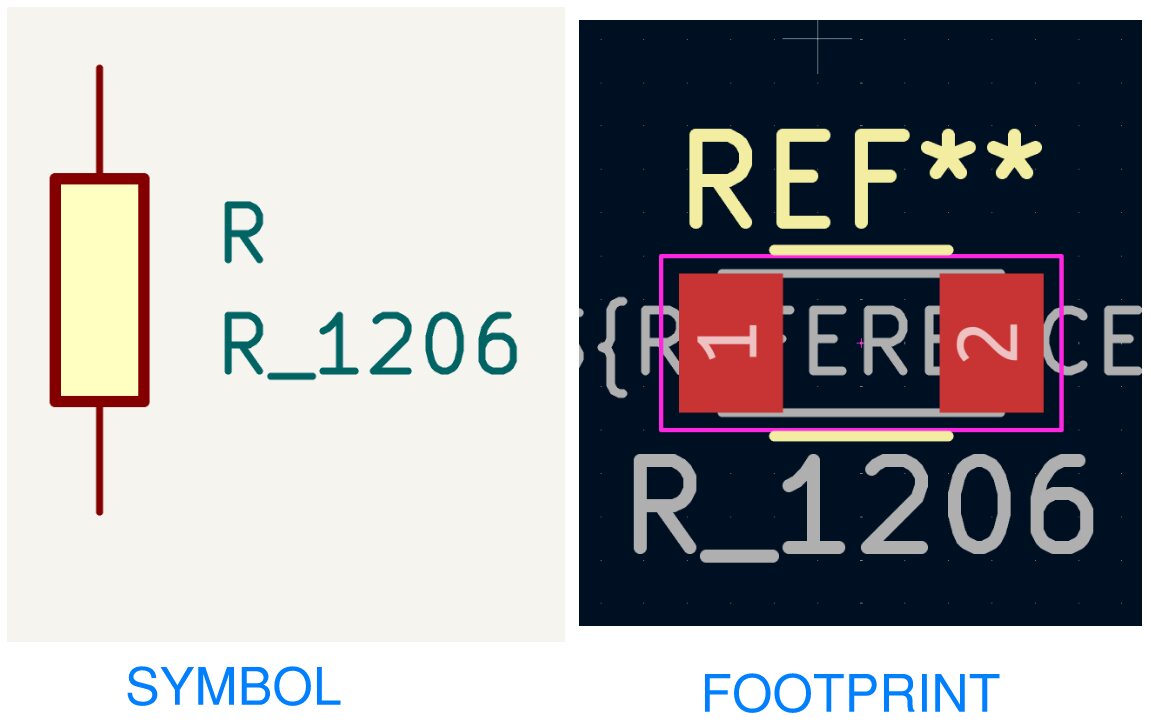 |
|:---------:|
| *Difference between Symbol and Footprint* |
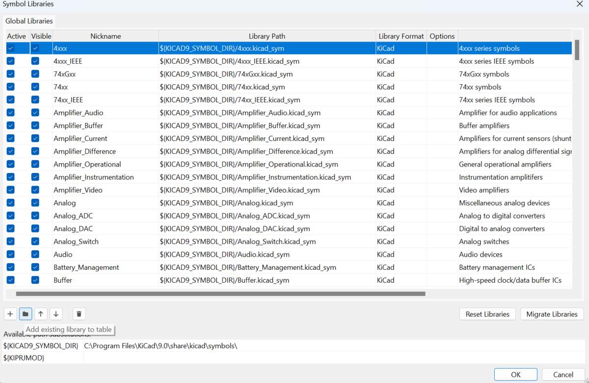
3. In KiCad, add the **Symbol Library**
|  |  |  |
|:---------:|:---------:|:---------:|
| *Go to `Preferences > Manage Symbol Libraries...`* | *Choose `Copy Default`* | *Click the folder icon at bottom to Add Existing, and add the file `fab.kicad_sim`* |
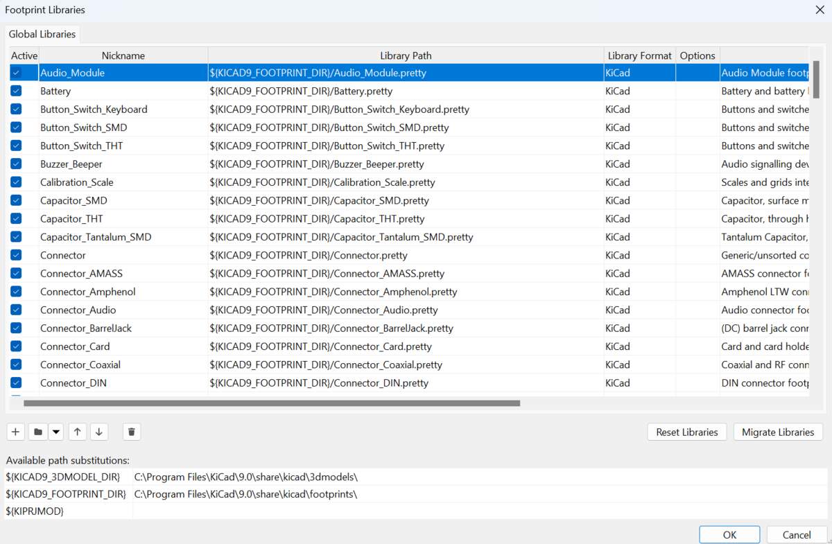
4. Do the exact same thing for the **Footprint libraries**
|  |
|:---------:|
| *Go to `Preferences > Manage Footprint Libraries...`, click on Folder Icon and add the `fab.pretty` folder * |
5. Create a new project
| 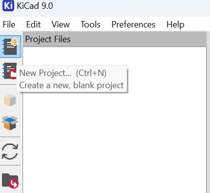 | 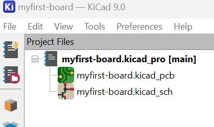 | 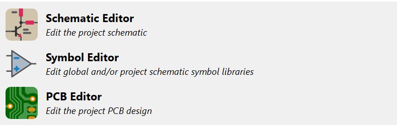 |
|:---------:|:---------:|:---------:|
| *Create a new project* | *You should see a new project show up here* | *You can now click on `Schematic Editor` or `PCB Editor` or any of the others to work on your project* |
KiCad shortcuts:
- `R` key to rotate a component.
- `U` key to select a whole wire in PCB Editor
Terminology:
- *Net* is the logical connection on Schematic
- *Wire* is physical connection on PCB
#### Understanding Pinouts
The chip vendor pin numbering is usually different from the Arduino Pin numbering! This can get very confusing.
Search the name of your board with the term pinout to find a diagram like this:
| 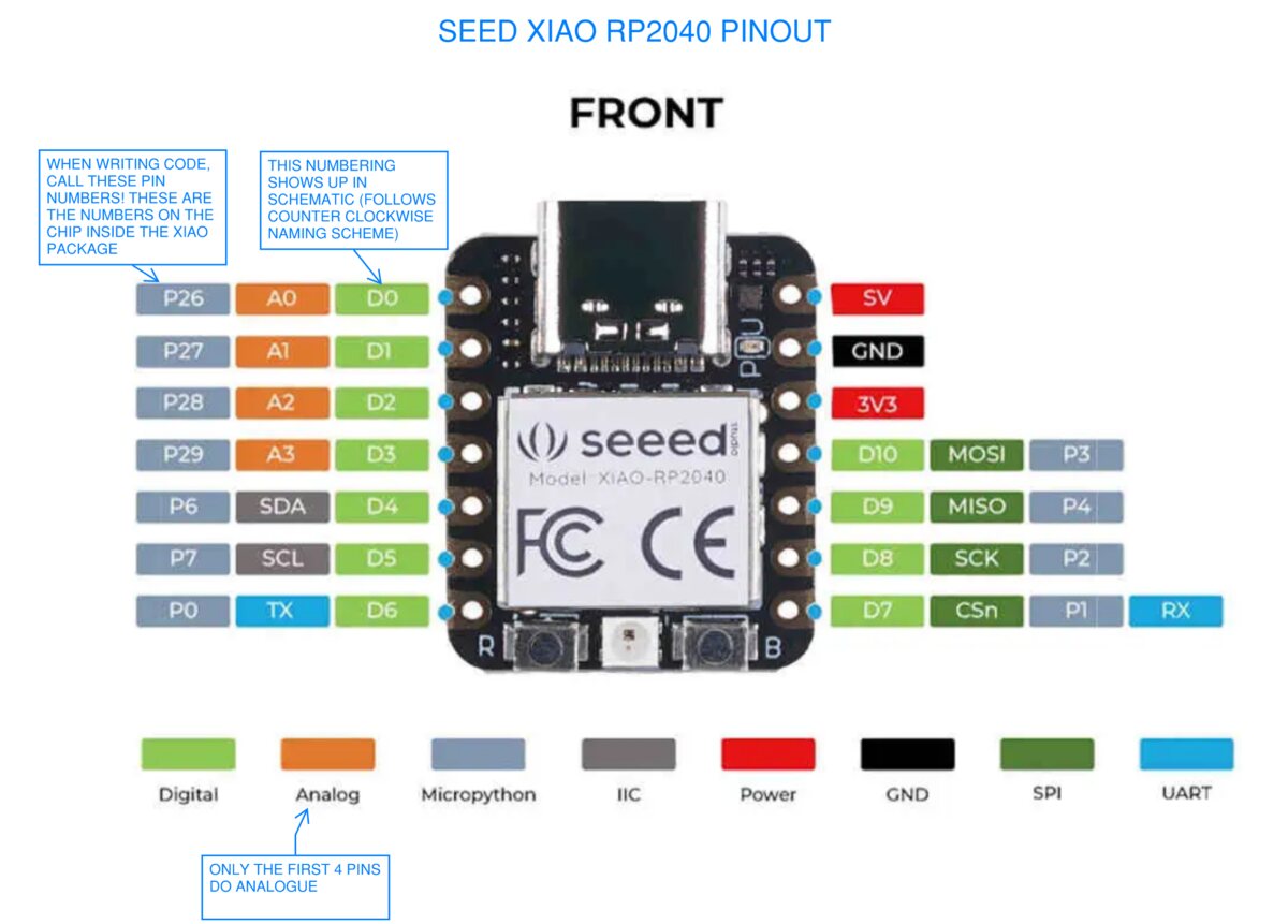 |
|:---------:|
| *XIAO rp2040 Pinout* |
Why is this? Because the XIAO package has one naming system, which is different than the RP2040 Chip which it contains.
You can reference the [Seed Studio XIAO RP2040 Schematic](https://files.seeedstudio.com/wiki/XIAO-RP2040/res/Seeed-Studio-XIAO-RP2040-v1.3.pdf) to understand how these pins are broken out in XIAO Package.
| 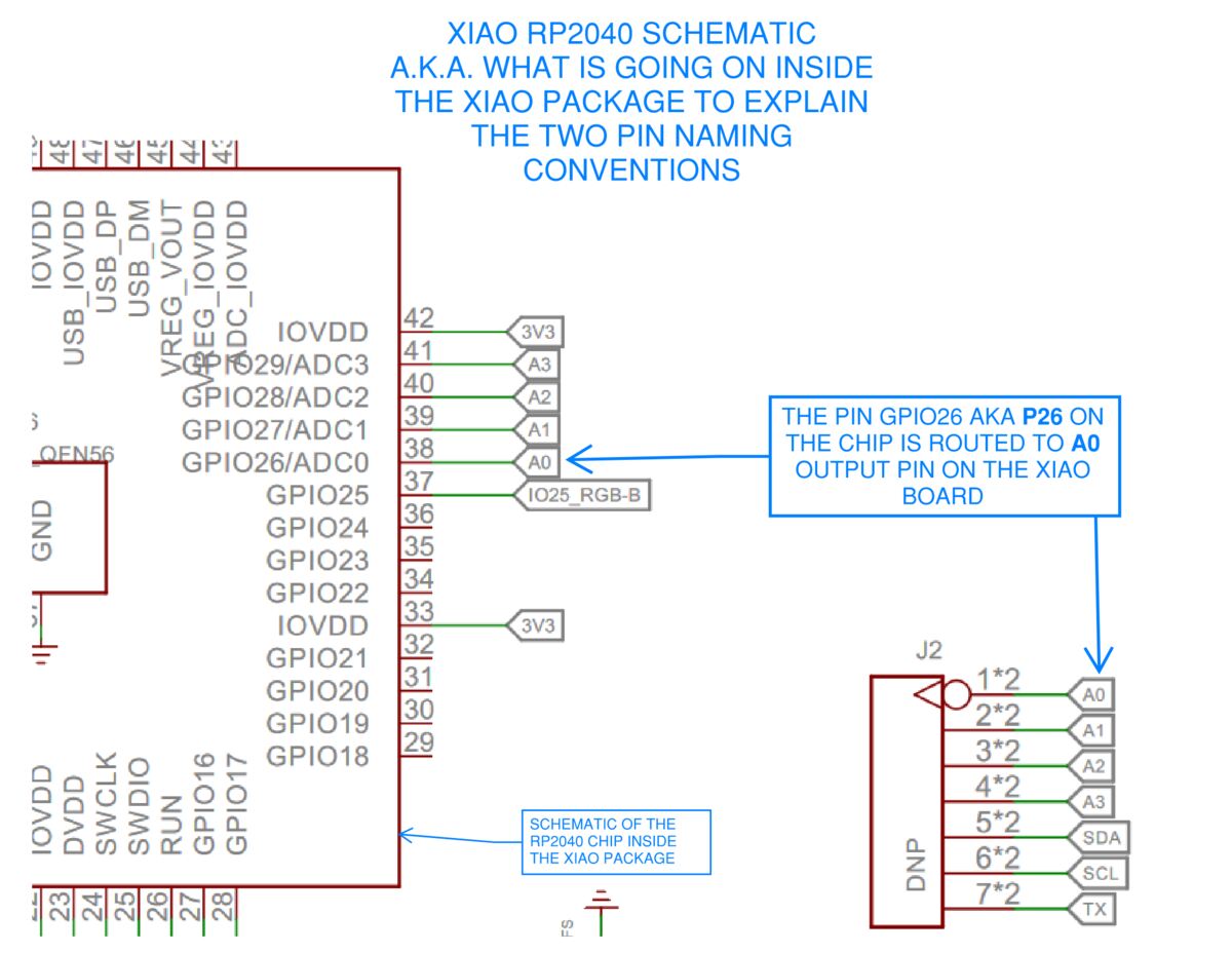 |
|:---------:|
| *Seed XIAO rp2040 Schematic* |
#### Components
##### Resistors
Always use 1206 size resistors for this class!
##### LEDs
Always use 1206 size LEDs!
#### Designing with KiCad
Here are the main commands/tools I used in KiCad:
| 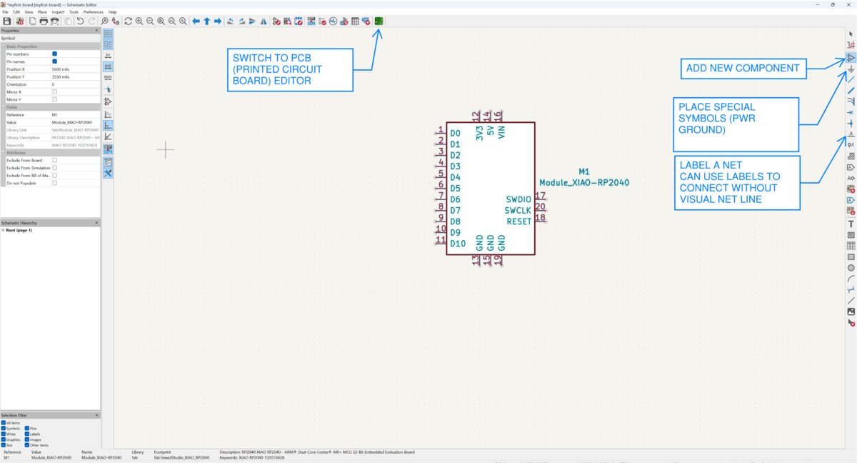 |  |
|:---------:|:---------:|
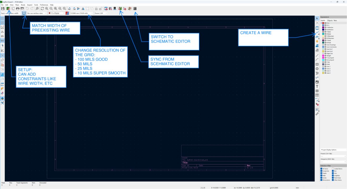
| *Schematic Editor* | *PCB Editor* |
##### Wire Thickness
Here is how to adjust wire thickness. I went with **0.4 mm** as Quentin suggests.
1. Go to `PCB Editor Board Setup > Constraints > Copper > Minimum Clearance` add 0.4 mm clearance
2. Go to `PCB Editor Board Setup > Constraints > Copper > Predifined Sizes` add 0.4 mm track width
| 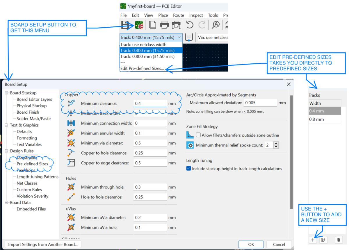 |
|:---------:|
| *How to Adjust Wire Thickness* |
Here is how to view & edit any symbol's properties, like it's footprint etc.
| 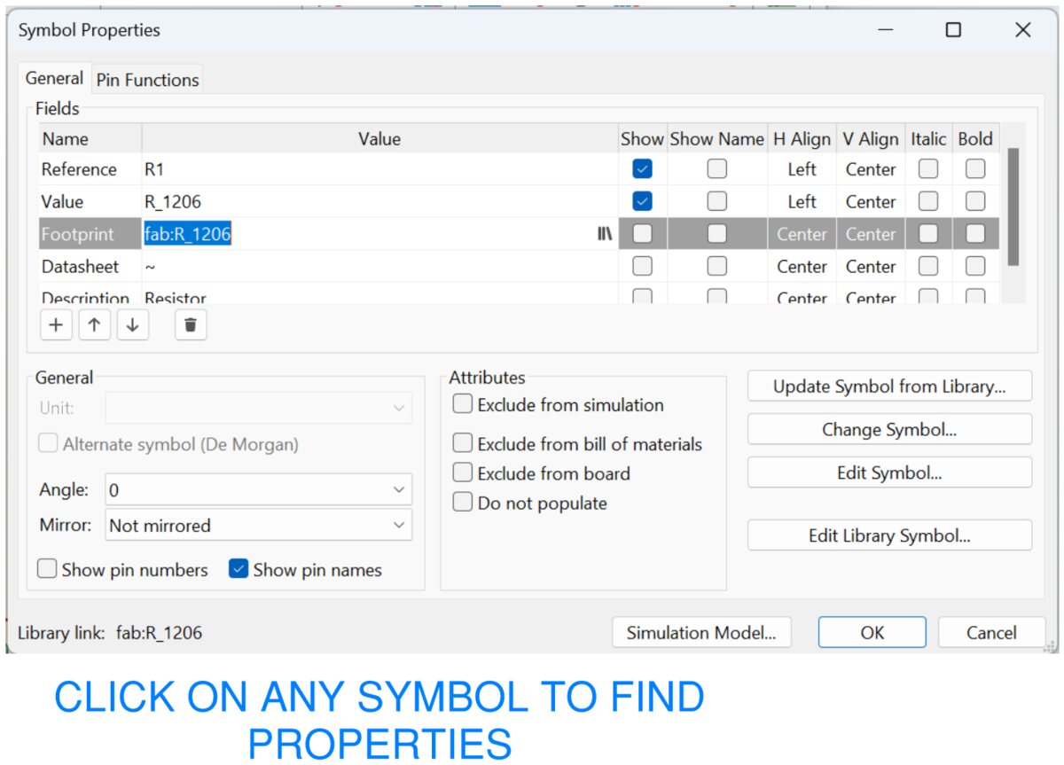 |
|:---------:|
| *View & Edit Symbol Properties* |
##### Adding Mounting Holes
You can add mounting holes by going to the `add part` in the PCB Editor and looking up `MountingHole_3.2mm_M3` or any other Mounting Hole.
##### Adding a poche or fill
This can also be helpful for making touch buttons on a device.
| 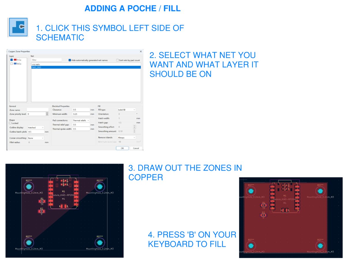 |
|:---------:|
| *Adding a poche/fill* |
If you want to connect any contacts from components to the fill, You will need a name for your net in the schematic editor before creating the poche fill in the PCB editor.
##### Rounding the Corners
In the PCB Editor, right click on a shape and look at Shape Modification > Round Corners/Fillet corners
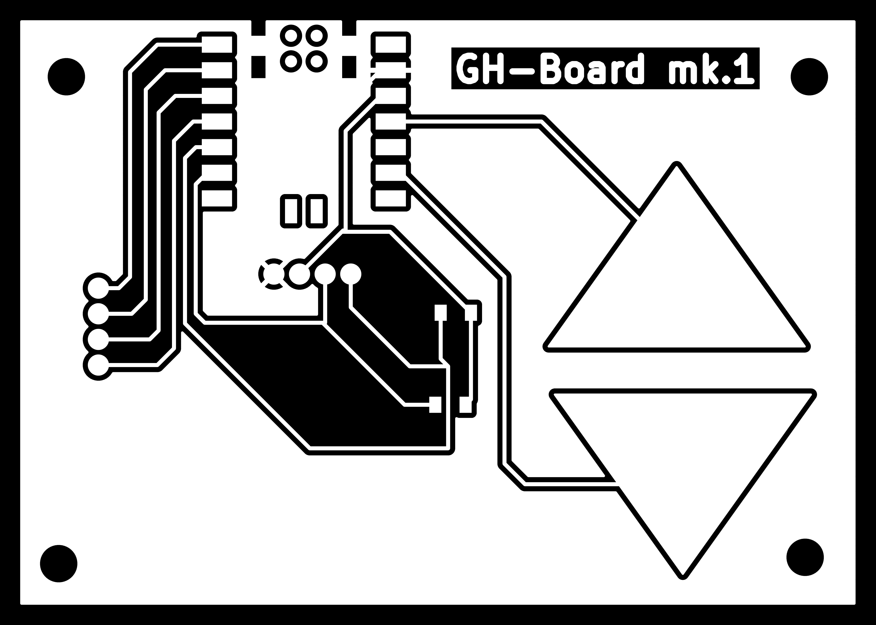
#### Designing an Analog Dev Board
I used KiCad to design an Analog Dev Board, that has the 4 analogue pin readouts accessible for any task, and two buttons and a screen for user input and feedback.
| 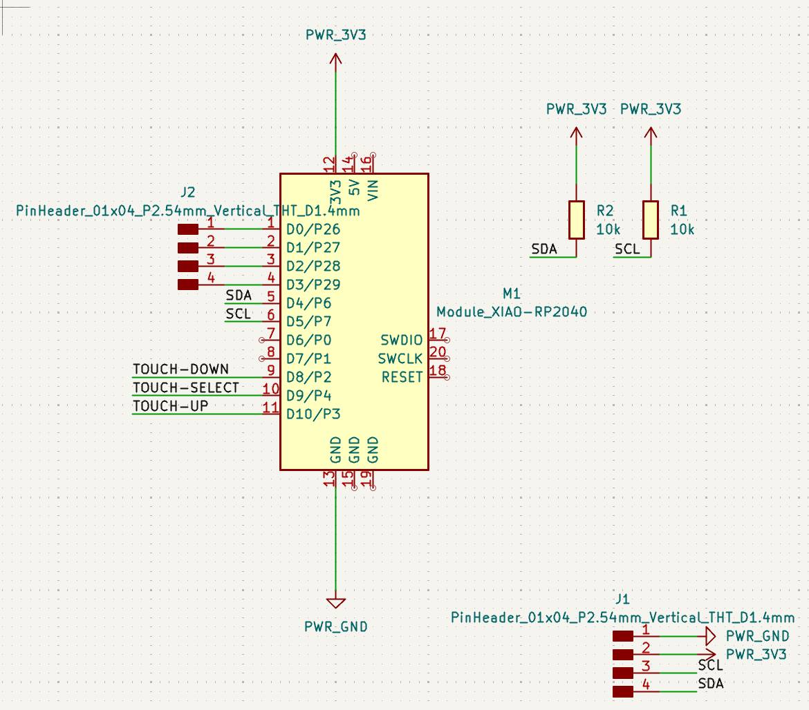 | 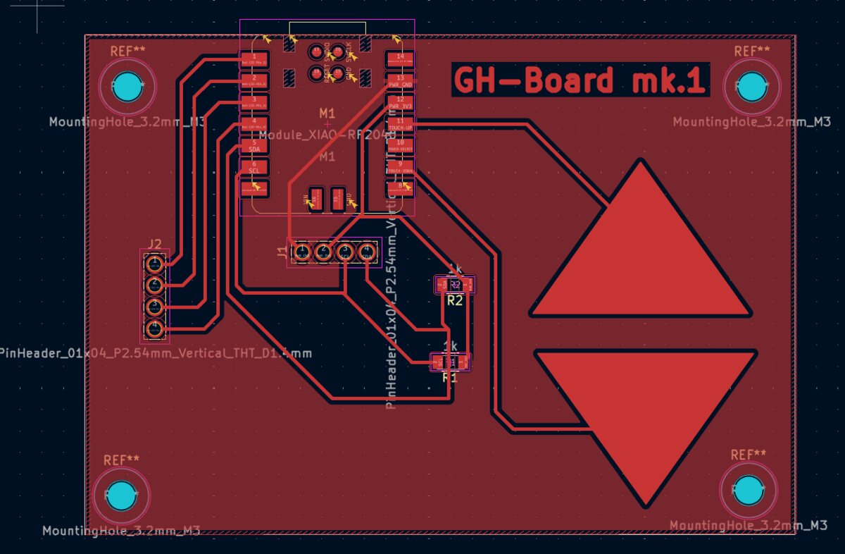 |
|:---------:|:---------:|
| *Analog Dev Board Schematic* | *Analog Dev Board PCB Design* |
Adding 3D models to the components:
- In the PCB Editor, click on a component to open Footprint Properties
- In Footprint Properties, go to the 3D Models tab
- Click on the little folder icon to add a 3d Model. You might see that there is already a path there.
Some important notes:
- Some 3d files might be in wrong orientation and need to be rotated using the fields on the left.
| 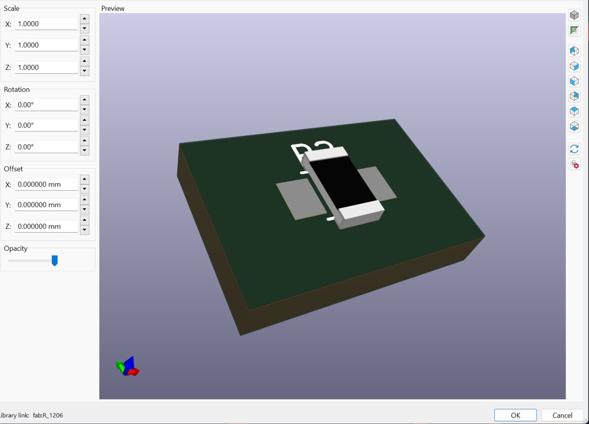 | 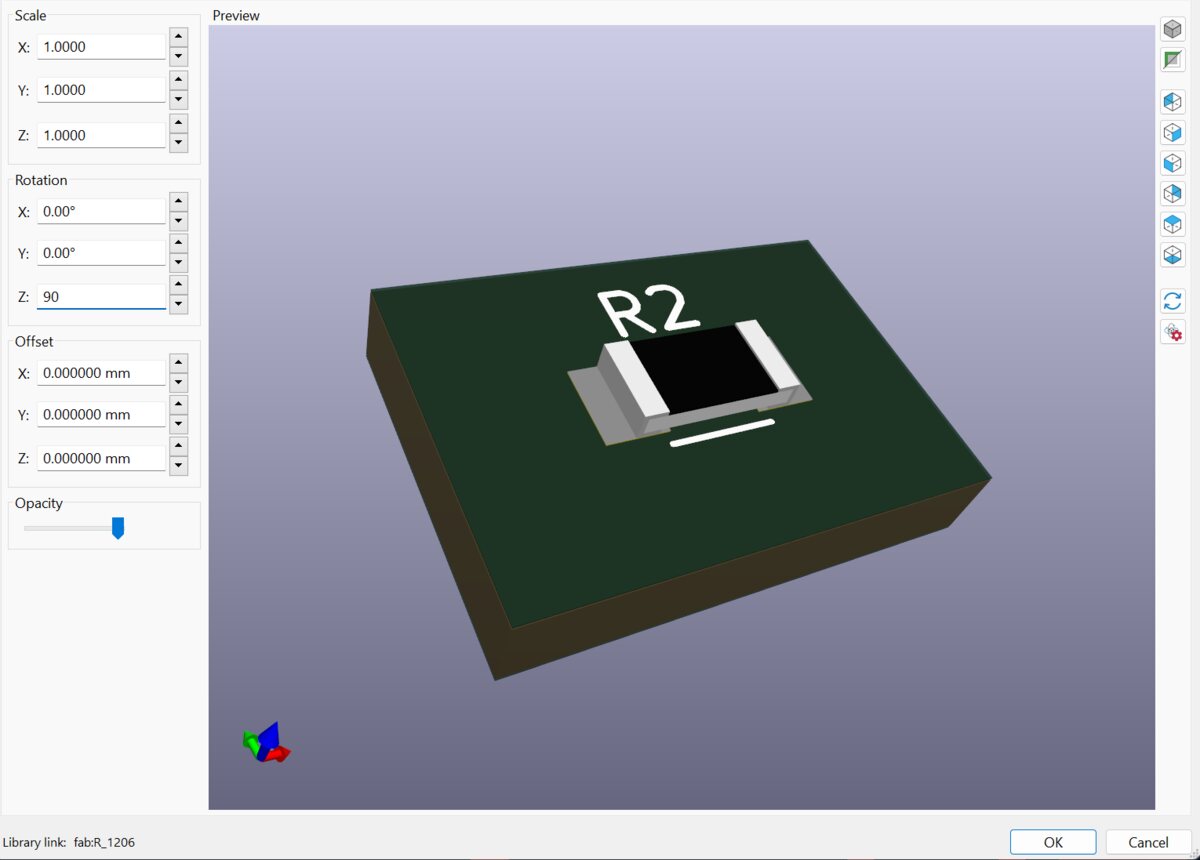 |
|:---------:|:---------:|
| *Resistor In Wrong Orientation* | *Resistor correctly rotated 90 degrees in the Z axis* |
- Note that for the Seeed XIAO there are two sockets: `Seeed_XIAO-Generic_InSocket_SMD.step` and `Seeed_XIAO-nRF52840_Sense.step`. You want to choose `Seeed_XIAO-nRF52840_Sense.step`
I had to do 180 rotation on the board to get it in the right orientation.
#### Designing the Board
Here is a 3d visualization with all the components added!
| 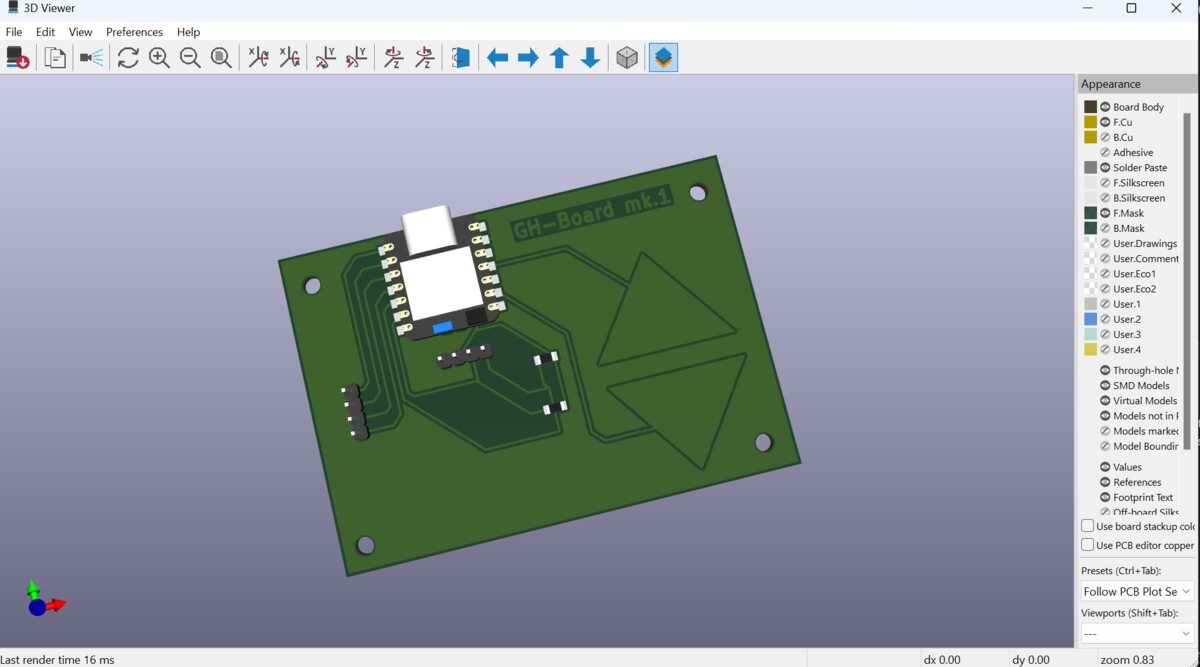 |
|:---------:|
| *3d view of rp2040 Analogue dev board* |
#### Exporting files
You can export by clicking on the plot icon on the top right (looks like a printer with legs).
| 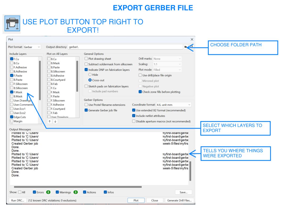 |
|:---------:|
| *Exporting Gerber Files: Click* **Plot** *and* **Generate Drill Files** |
1. Make Sure `F.Cu` is selected to cut traces on the Front
2. Make sure `Edge.Cuts` is selected to cut edges and holes
3. You can choose to select or deselect `F.Silkscreen` if you want documentation to know where the components go (we can't silkscreen here because the process is super toxic)
4. Click `Plot`
5. Click `Generate Drill Files...` will give you the places where you need to drill. This is very important!
I used [gerber2img](https://quentinbolsee.pages.cba.mit.edu/gerber2img/) written by Quentin to turn my gerber files into images that the machine can cut.
Here is the process:
1. Drag and drop your copper traces gerber file first.
2. In the Settings on gerber2img, LOCK the origin and the dimensions. This is very critical. *It is key to have these settings locked and to keep all of them the same so that when you add the drill holes or the outline everything lines up* You can also set the margins to 0, 0 if you want, or have a small margin.
3. Select Black and White in the settings
4. Click Download Render at the bottom of the page.
5. Add your drill path gerber file, and click download render, making sure that origin, dimensions and margin are the same.
6. Do the same for the outline, making sure that origin, dimensions and margin are the same.
|  |  |  |
|:---------:|:---------:|:---------:|
| *Copper Traces to Engrave* | *Holes to Cut* | *Edge of Board to Cut* |
> Extra credit: try another design workflow
> Extra credit: design a case
## Attachments
[RP2040 Analogue Dev Kit Copper Traces PNG](images/251015-analogue-rp2040-kit-traces.png)
[RP2040 Analogue Dev Kit Holes PNG](images/251015-analogue-rp2040-kit-holes.png)
[RP2040 Analogue Dev Kit Outline PNG](images/251015-analogue-rp2040-kit-outline.png)
[Gerber files](files/myfirst-board/gerber)
## Acknowledgments
Gert for running the TA group session and showing us how to use the instruments.
Quentin for the recitation on Kicad, for which much of the information on KiCad, schematics and board design comes from.
Anthony for helping me import the correct libraries on Kicad.