Week 8
Assignments: Input Devices
...pending
Assignments: Input Devices
group assignment:
probe an input device's analog levels and digital signals
individual assignment:
• measure something: add a sensor to a microcontroller board that you have designed and read it
Light Sensor and Dimming
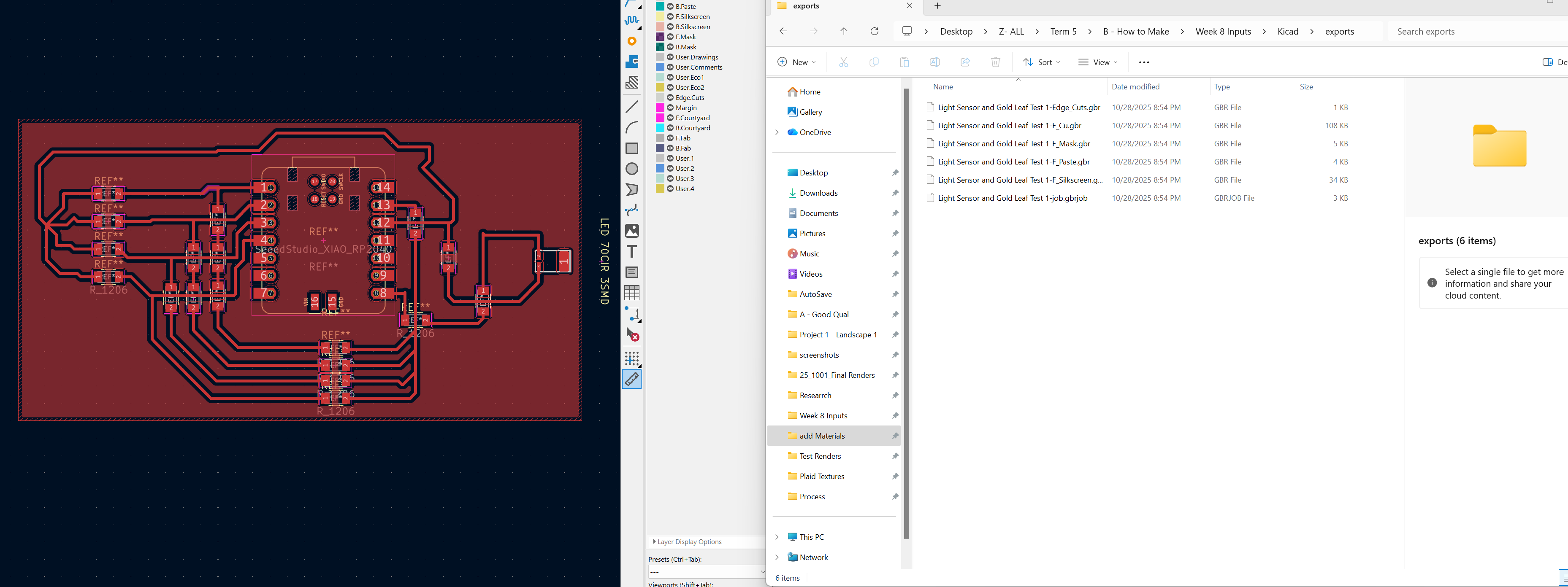
KiCad file is here: file
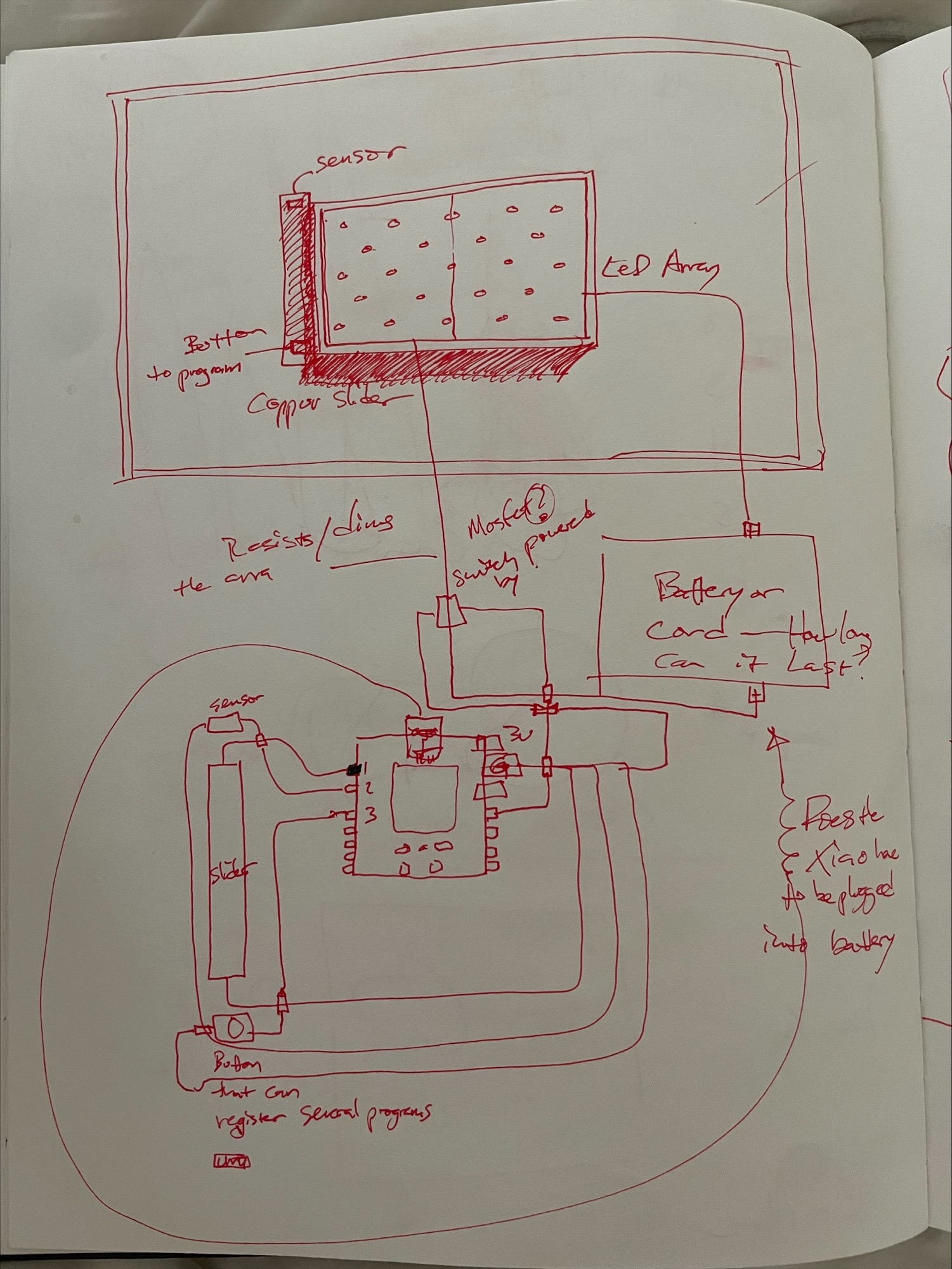
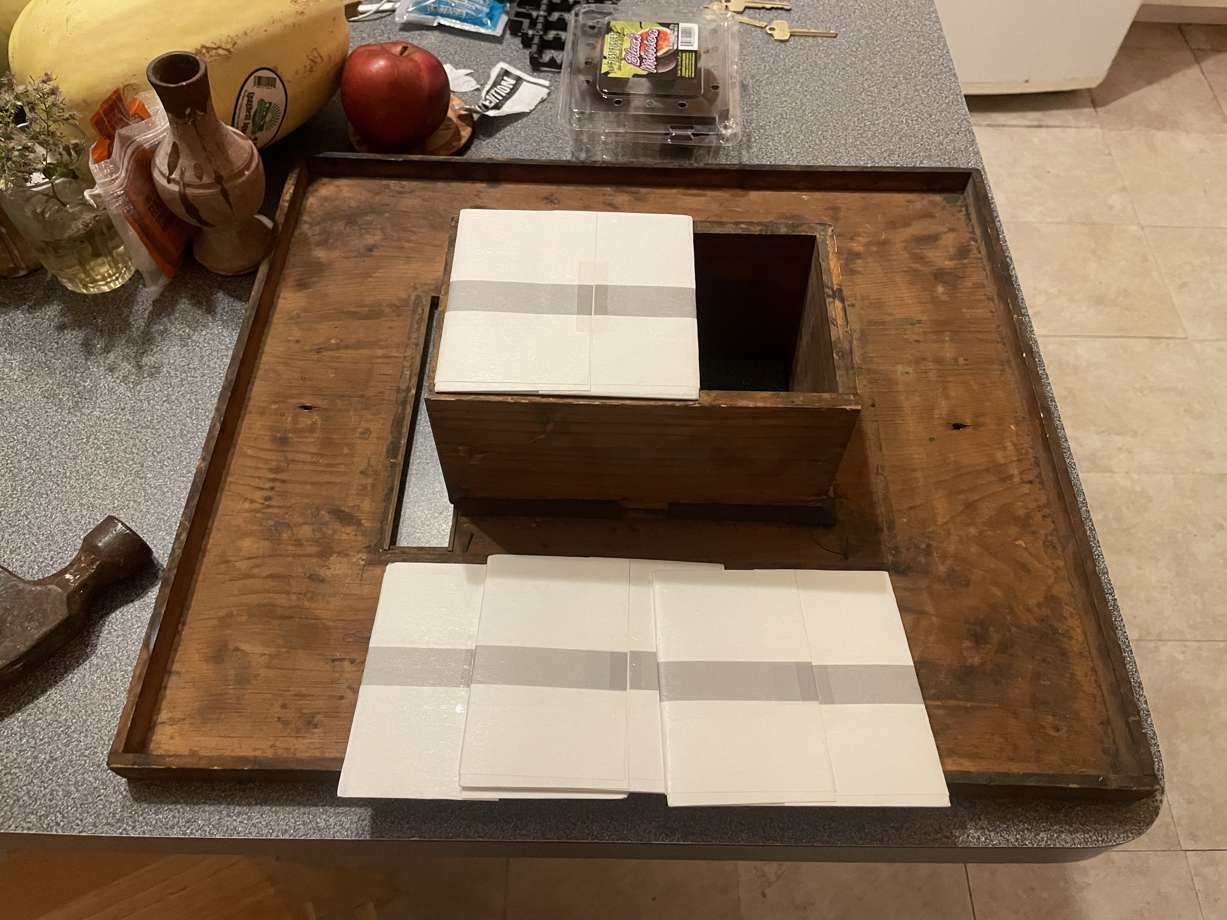
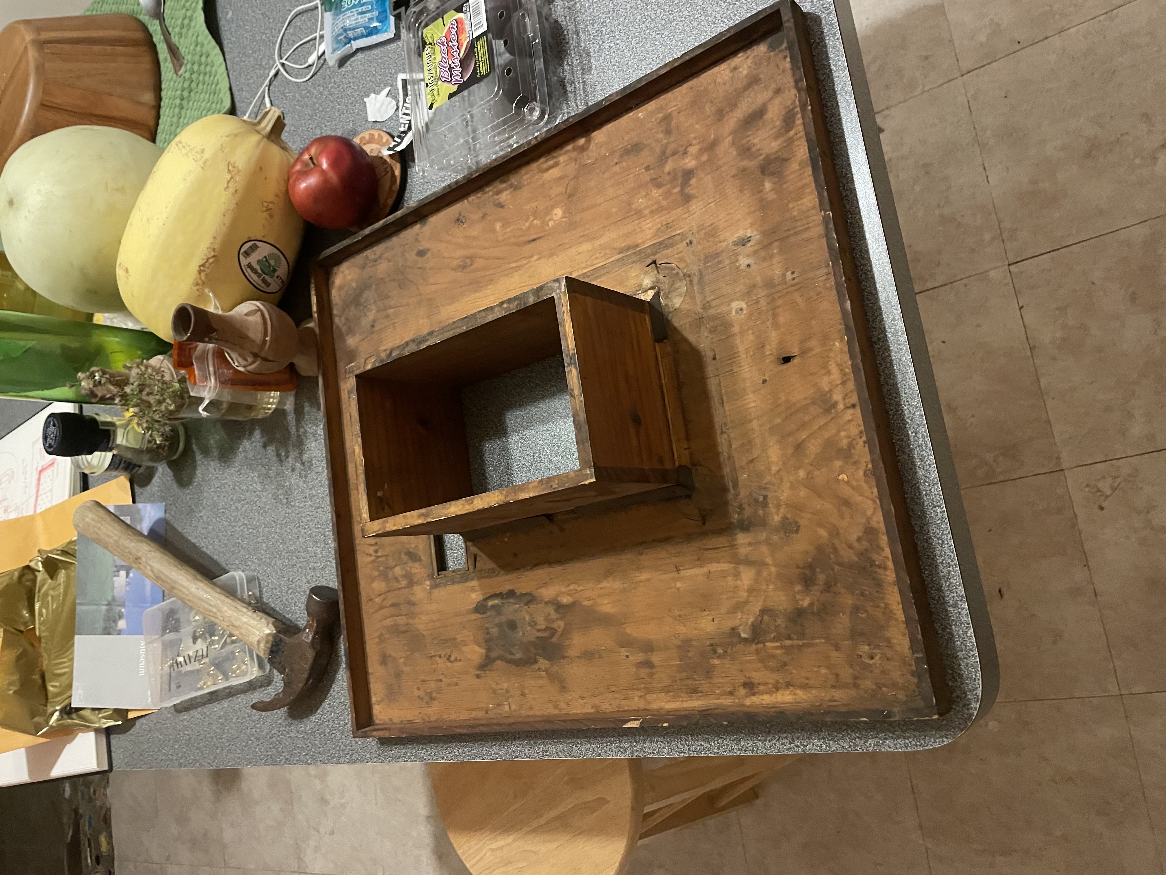
This week I set out to make a major move toward my final project, which involved mocking up a gold leaf test plate between two glass panes, paired with a super-bright LED array and a light-sensing input system. The goal was to create a micro-controlled LED module that reads the ambient light conditions in the room—whether interior light, indirect sun, or direct sun striking the panel—and outputs an equivalent level of LED light back into the space. In short: a feedback-based light collector that emits the same amount of light that hits it.
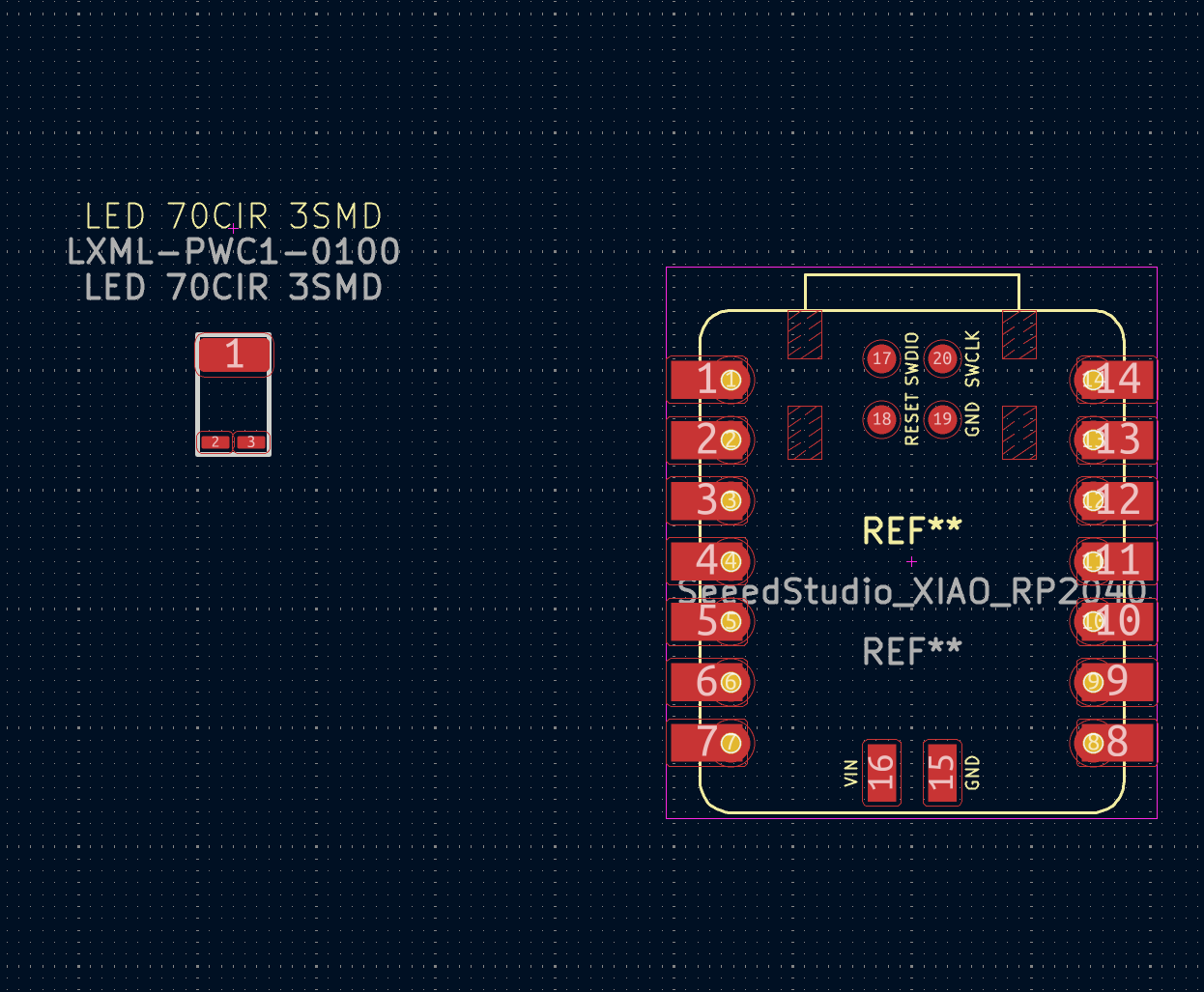
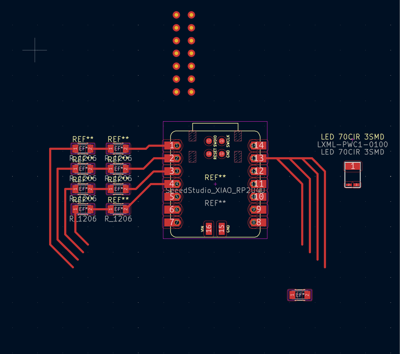
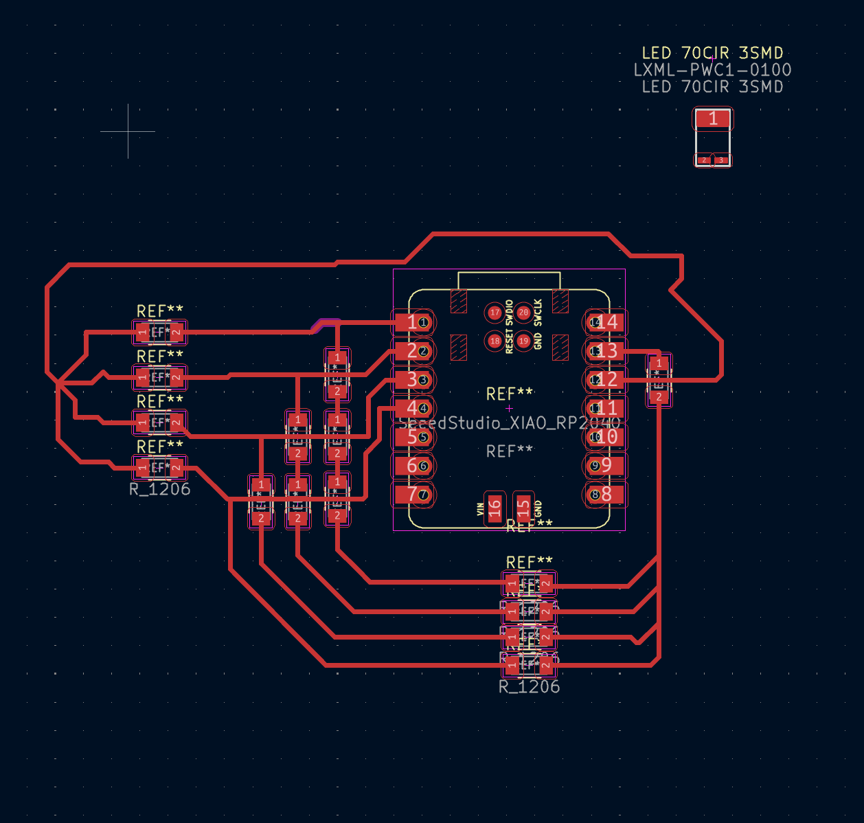
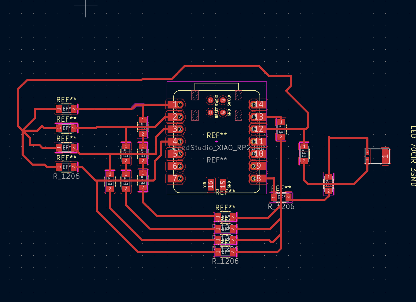
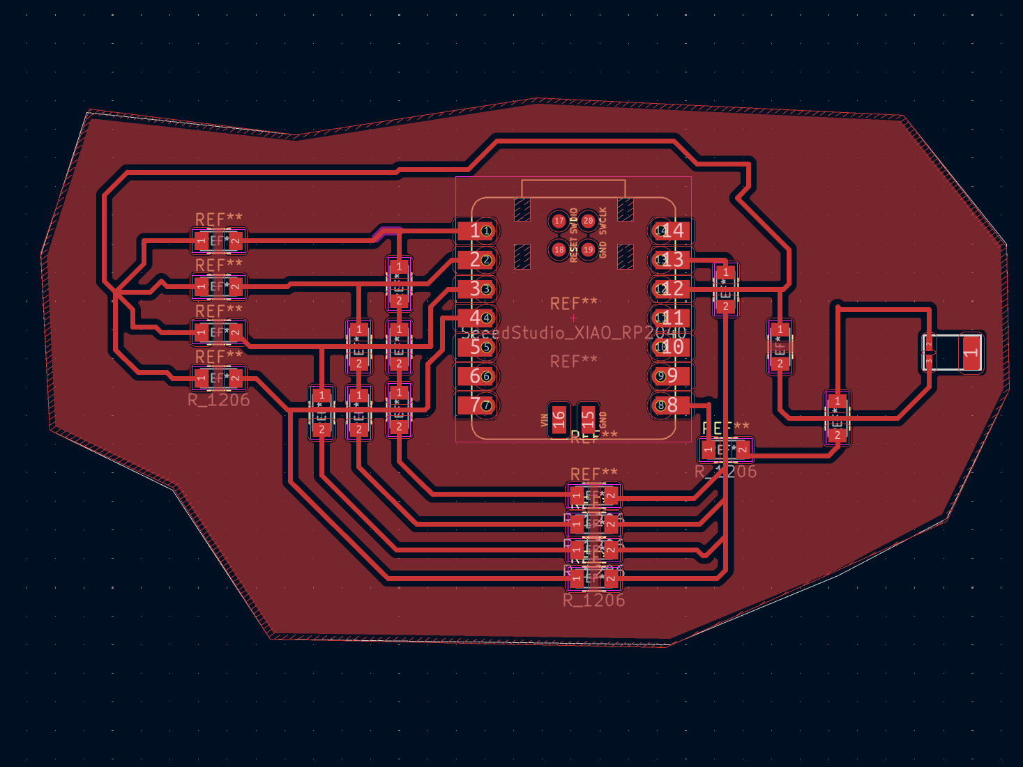
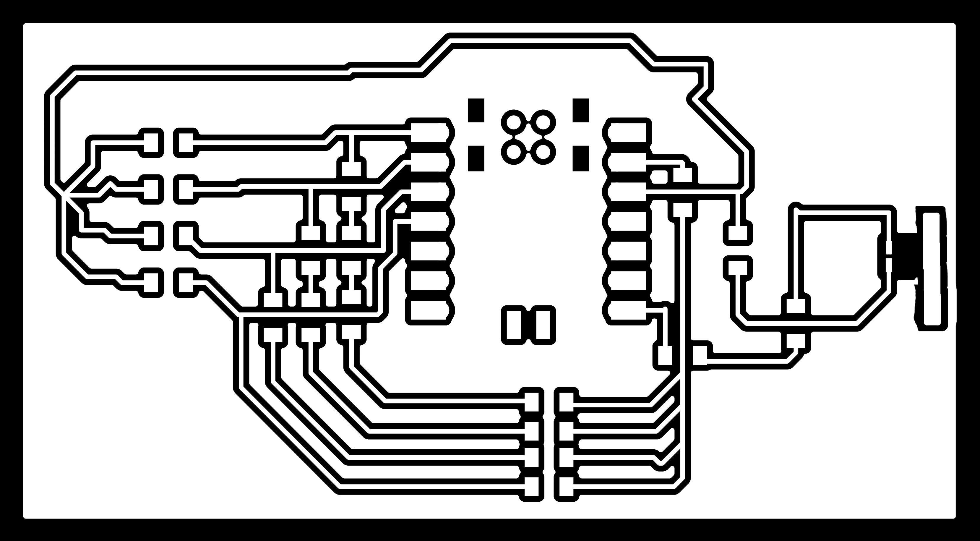
I worked with Anthony to design a system using four photoresistors, each wired with a different resistor value and assigned to one of the four analog pins on a Xiao 2040. This was necessary because the light range hitting a window-mounted panel is extremely wide, and a single sensor cannot accurately capture dim to bright conditions. By giving each of the four sensing circuits a different resistance range—from around 2.5 ohms to several hundred—we can collectively measure a full spectrum of ambient light and produce a proportional LED output from dim to very bright.
The whole assembly is intended to fit inside a wooden table-saw box. This object is an antique casting jig used to mold metal parts for table saw equipment, and its geometry makes it an ideal light box enclosure. The open slot where the blade would normally sit is the perfect location for the sensor array, along with a stepped capacitive-touch dimmer interface. I want as many touch steps as possible across this aperture—both for visual effect and for user experience—essentially a copper-band gradient along the length of the saw slot. After using the four analog pins, that leaves six data pins for the touch interface, excluding the one reserved for the LED array.
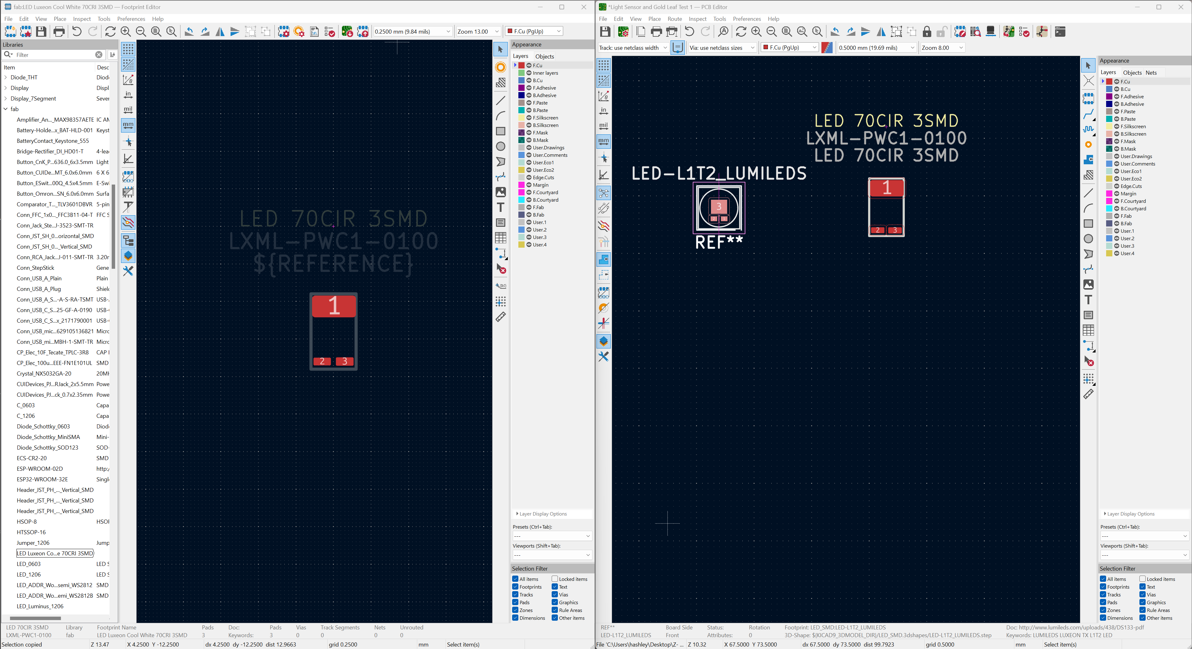
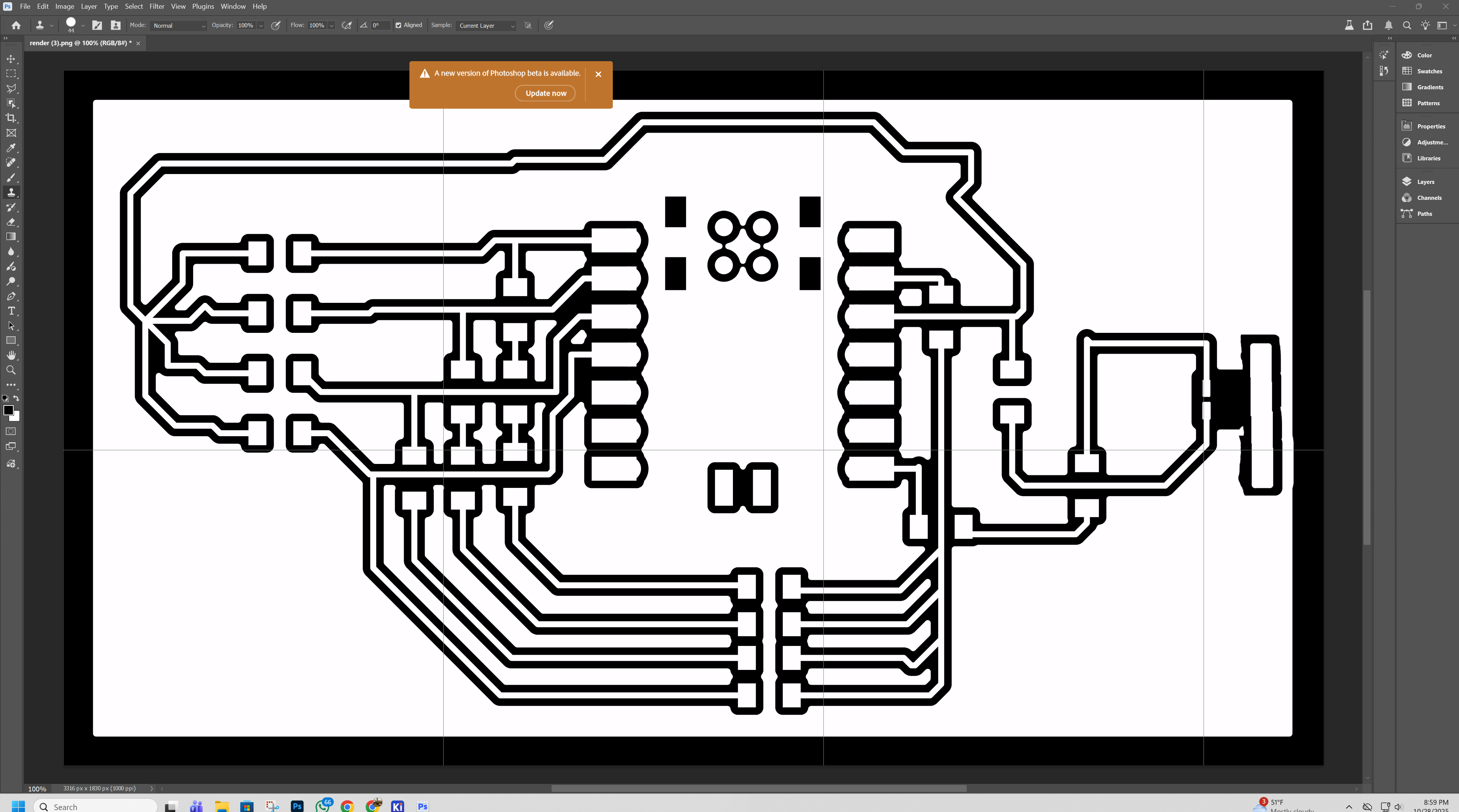
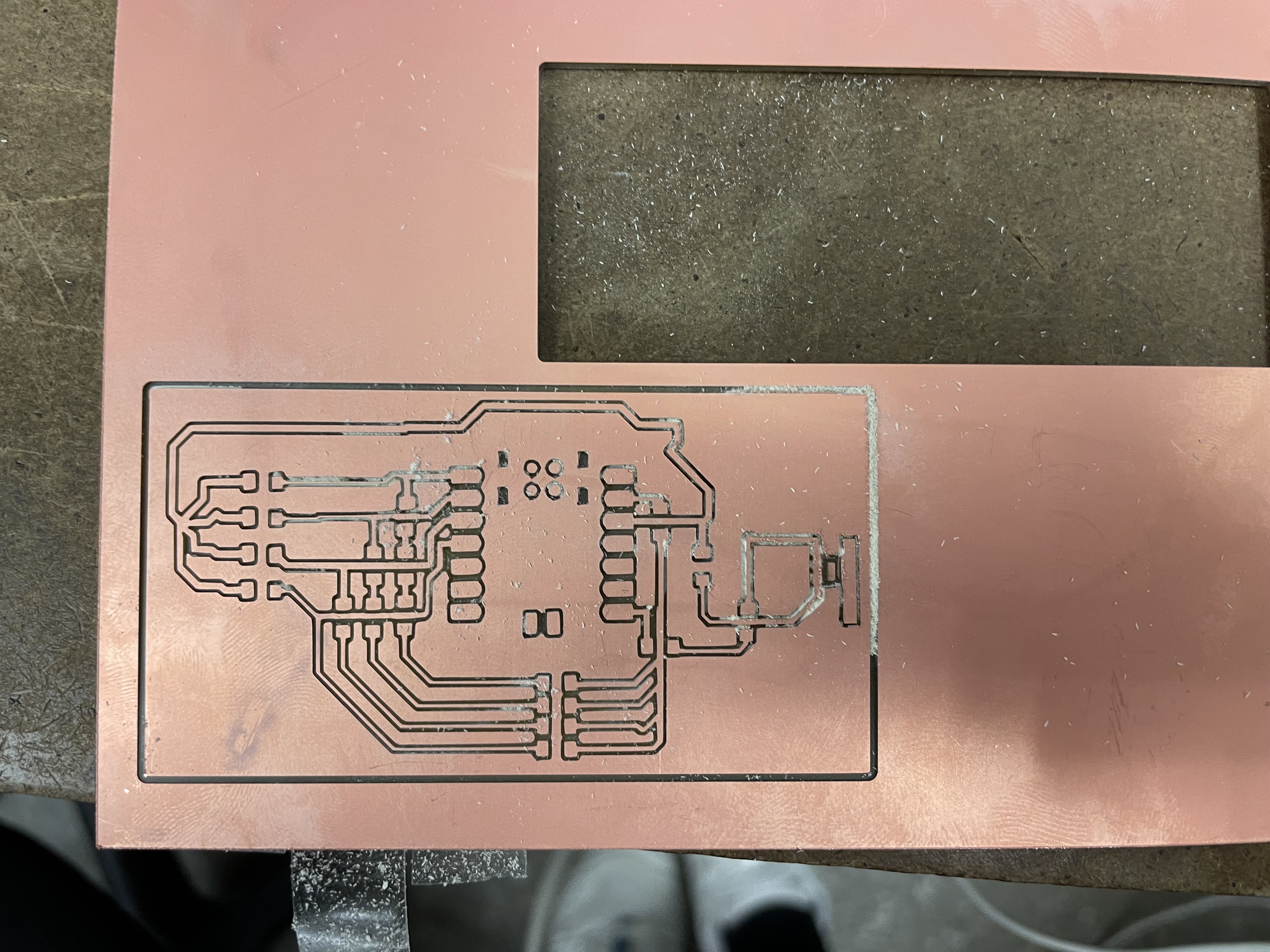
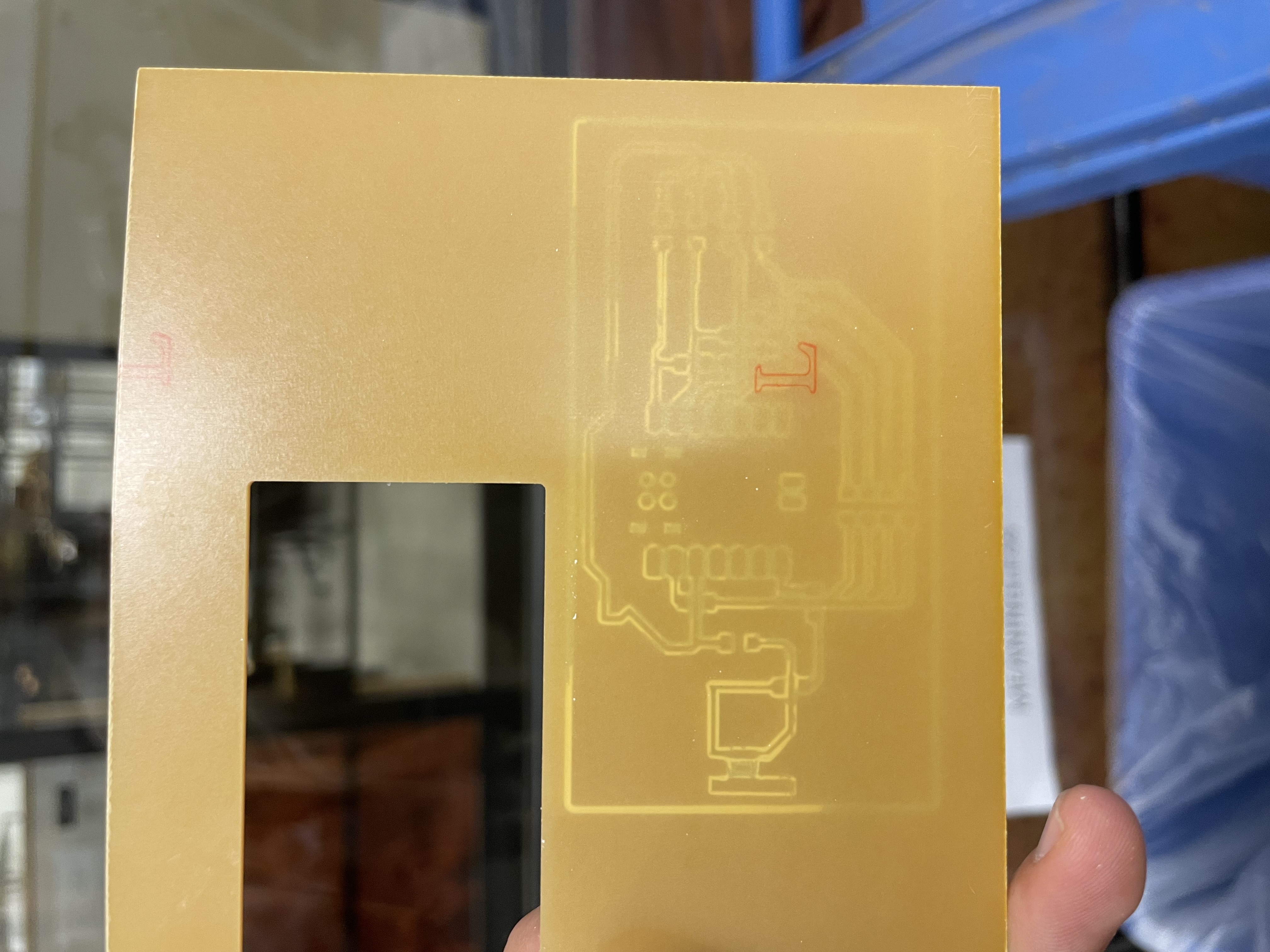
The LEDs are a set of extremely bright components that Anthony gave me. They required a custom footprint, which I designed this week, and I milled a small PCB plate as a test. The idea was to prototype the LED array and confirm spacing, heat concerns, and solderability before committing to the full panel version.
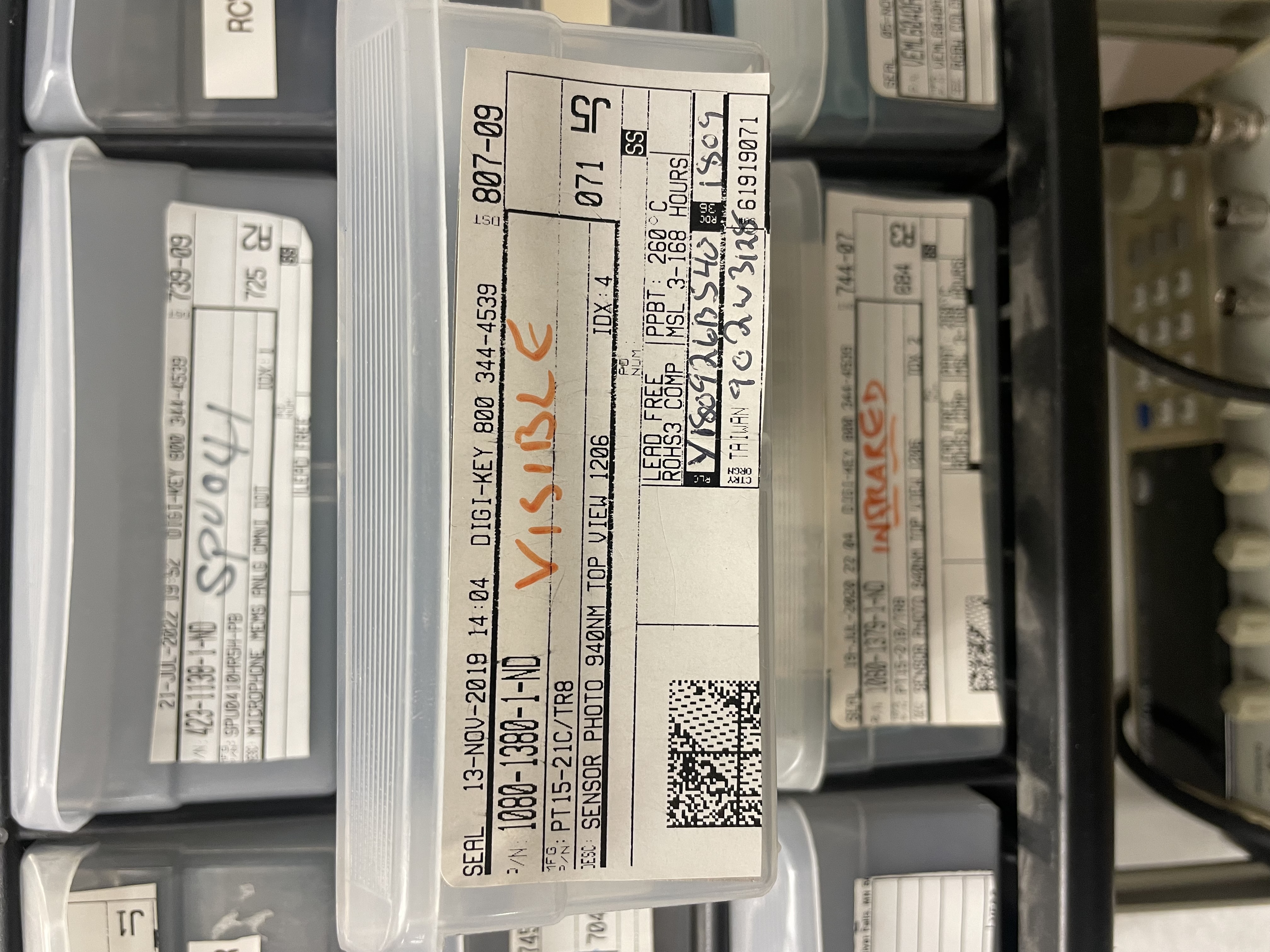
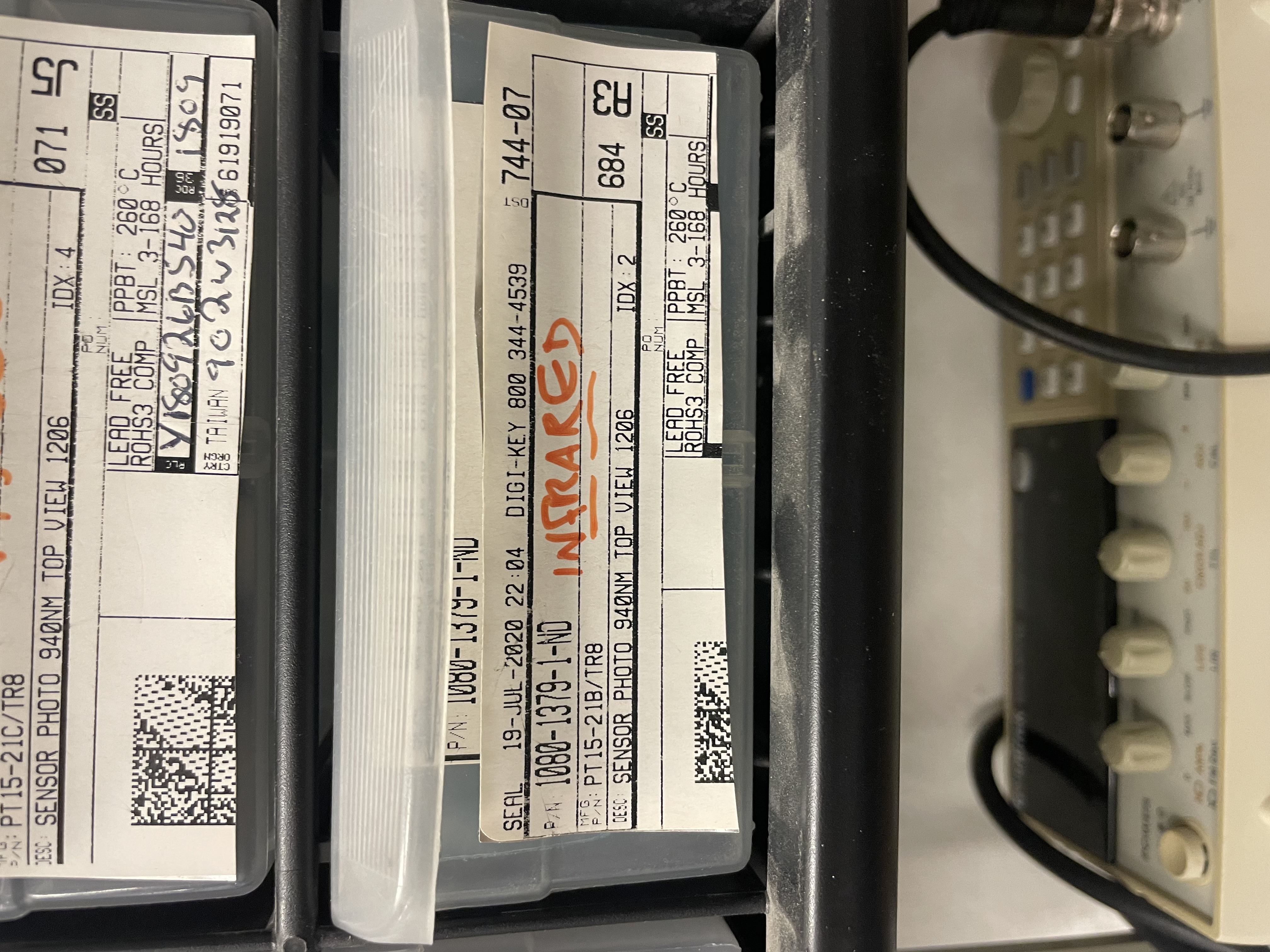
In producing the PCB, I ran into a number of issues—mostly time and tool-related. I assumed the shop would have the photoresistors I needed, but the only parts available were phototransistors, which require different wiring logic. This forced me to redesign the board in KiCad. I also struggled with the Fab Library, since many of the components I needed were hard to locate, so I ended up skipping the schematic stage entirely and worked directly in the PCB layout tool.
When I milled the board and attempted to solder it on Tuesday, I realized the cut was too deep. There was likely dust and two layers of tape stuck to the back of the PCB during milling, which caused the traces to lift and tear as I soldered. After repeatedly repairing lifted copper, I quit for the night—partly because the board had become unusable, and partly because I was exhausted and it wasn’t worth sacrificing more sleep for a test plate.
The plan for the coming week is to update the design to include both input and output functions on a single PCB, satisfying both assignments at once. I’ll produce the four-step photosensor array, integrate a milled capacitive-touch interface, and aim to get a dimmable light output running from the same board. More to come—I didn’t accomplish as much as I hoped this week, but it has been overwhelming. I’ll push forward this coming week.