Introduction
This assignment resumes the electronic design from last week, and we are going to use a milling machine to produce the PCB board. Last week, because of the limited time, I just designed a very simple PCB for XIAO RP2040. However, I want a uniform platform with as many I/O ports as I can, because I’m going to use it to control several motors. As a result, I changed to Raspberry Pi Pico W, which also uses the RP2040 core but has more I/O ports. Also, last week I watched and learnt from the EECS section recitation for fusion, but I also want to learn KiCAD. So I relearned KiCAD from the CBA section.
1) EDA:
The general idea is to design a developer board for the Raspberry Pi Pico W. I plan to add a screen to show information, four buttons to interact, bring out as many pins as I can, and include the power input/output connectors. Here is the pinout setup of Raspberry Pi Pico W. VSYS is the input power connector, and VBUS can output 5V DC/ 3V3(out) can output 3.3V DC. When RUN pin is shortened, the whole system will shut down, so it can connect to a button for reset function. 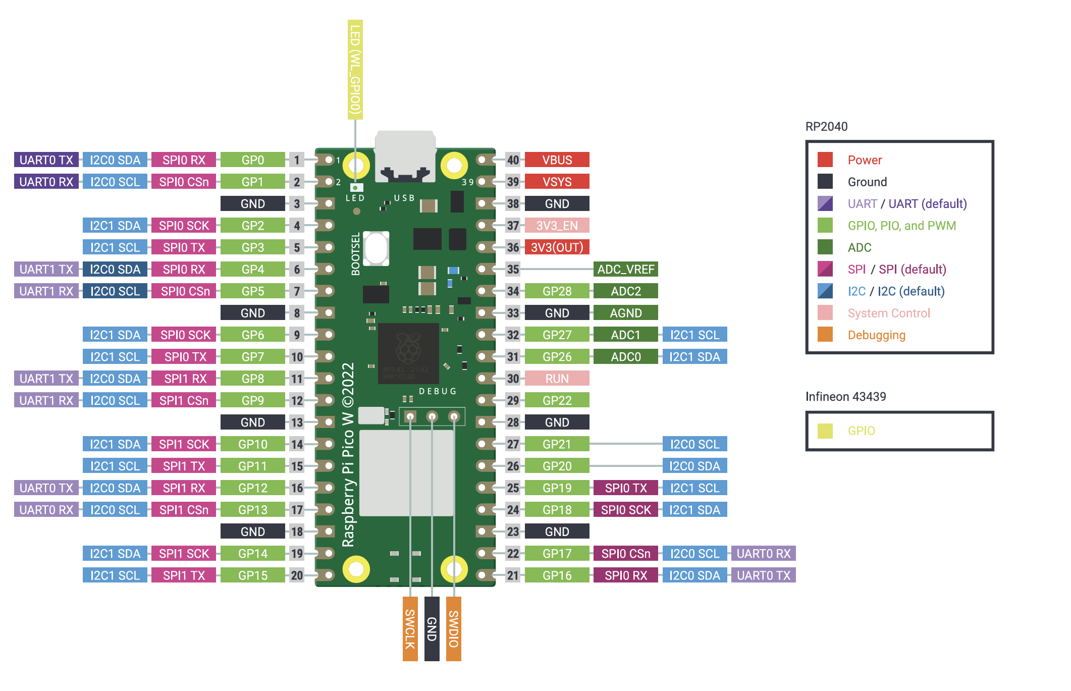
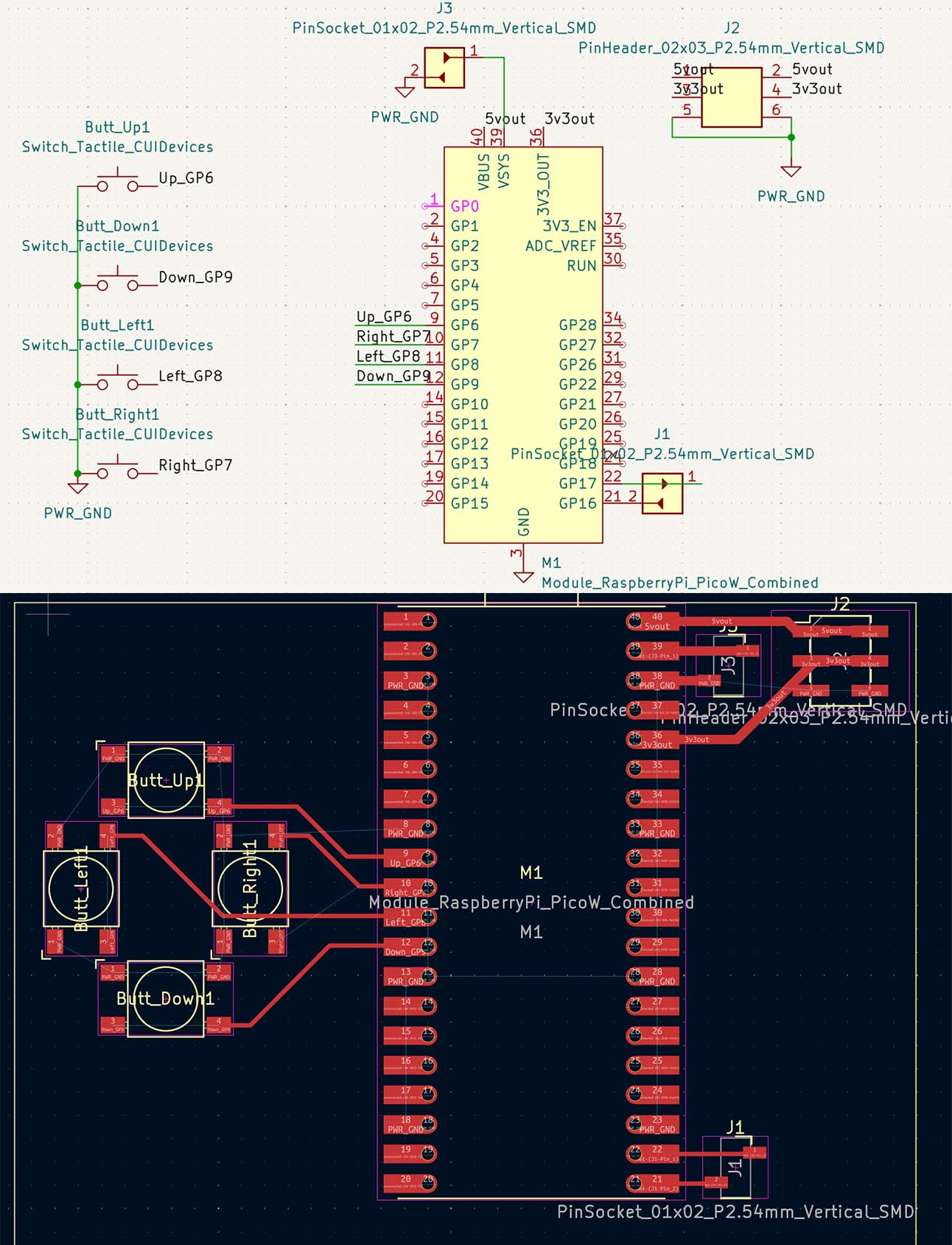
The primary result looks like this in the beginning: (Hasn’t added the pinout parts)
At that time, I didn’t realize the problem was:
I chose the wrong button with a different size (too big) when compared to the buttons in the CBA stock
The power input didn’t include the reverse connection protection
It’s also not in stock for PinSocket 1*2 with two pins at different sides
Didn’t consider where to put the screen
These problems will show up during my PCB production:
2) Bare Copper board production (Milling):
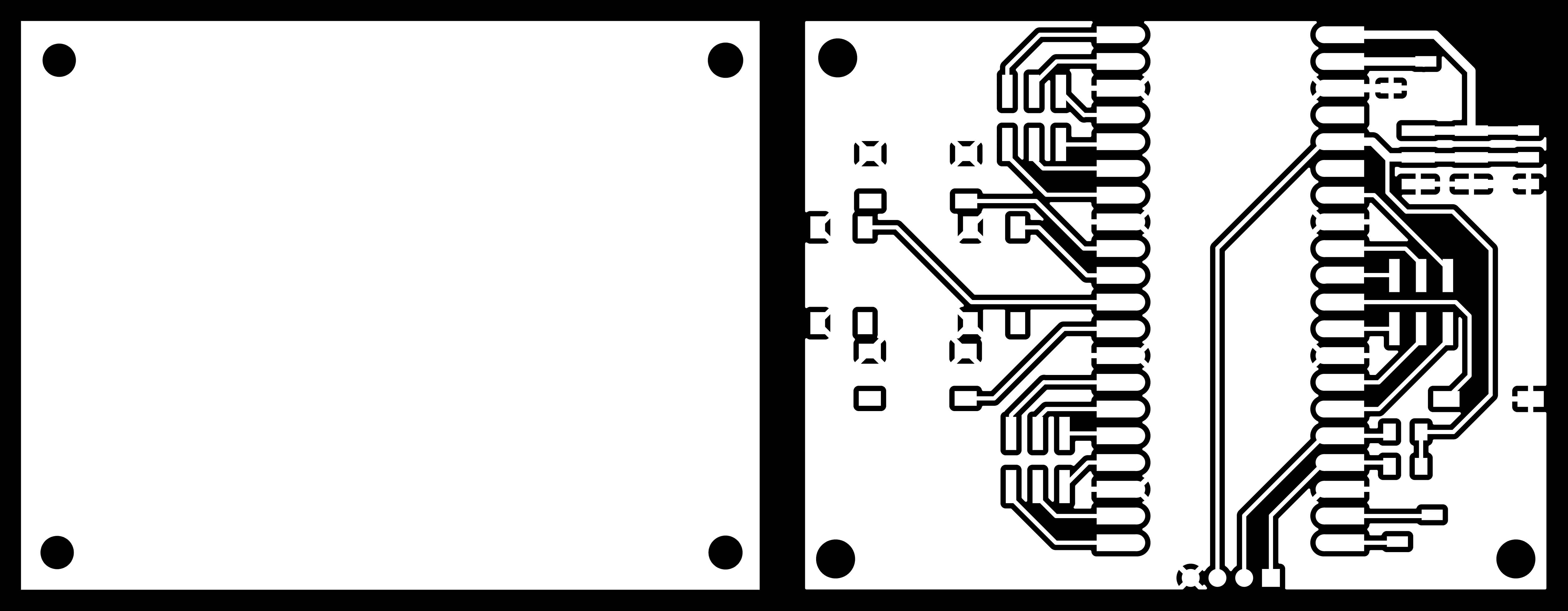
These are the files for my first milling PCB attempt. There is a very big problem inside, but only after it’s finished, I find it. The problem comes from the Gerber2img software. When I generate the image for trace and edges, I didn’t lock the size and position of them, so they have a relevant offset, which means both edges and holes are not aligned for the two milling stages. Also, I forgot to drill the small holes for the pins of the OLED screen.
To be honest, apart from this software-level bug, the milling process went pretty well: 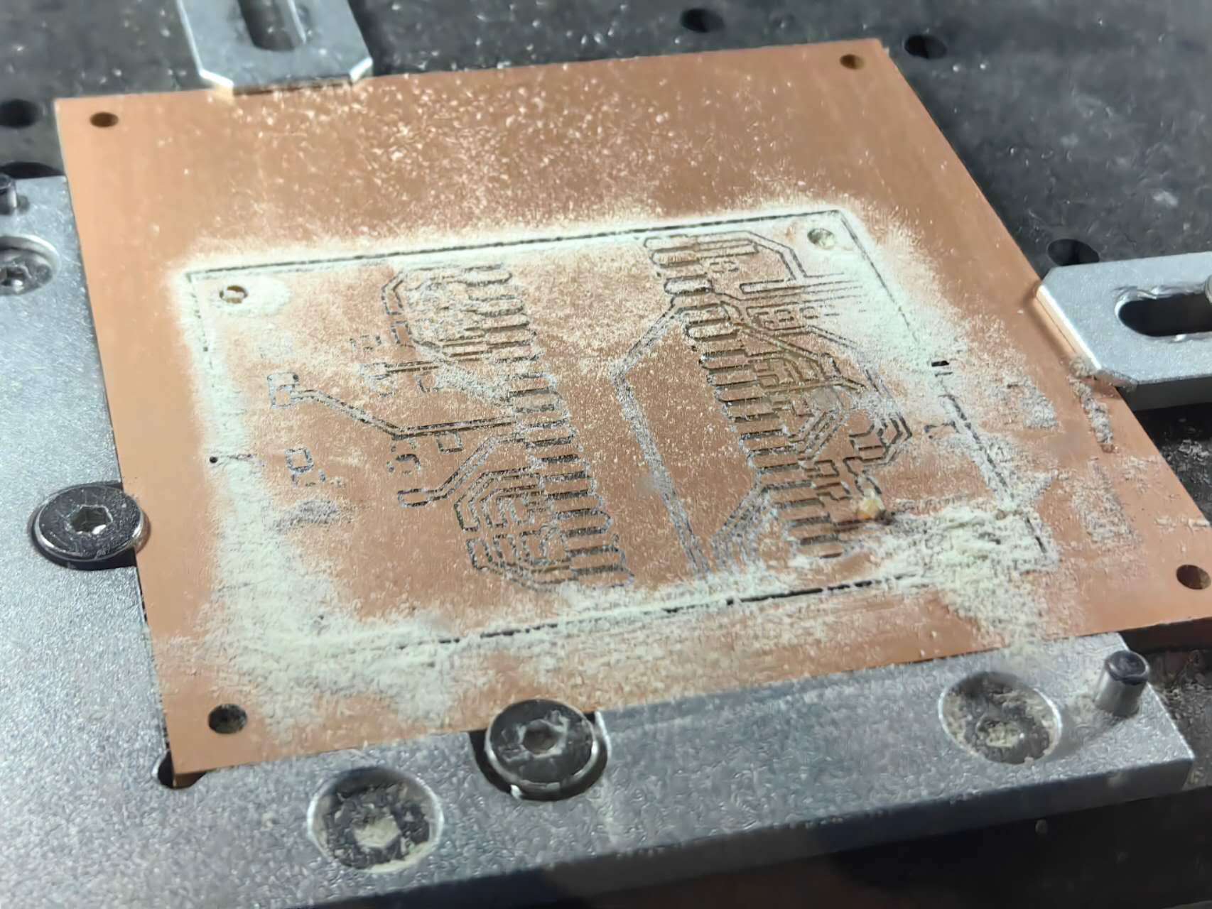
Even without sandpaper polishing, the traces are super clear and clean. And the offset I mentioned looks like this:
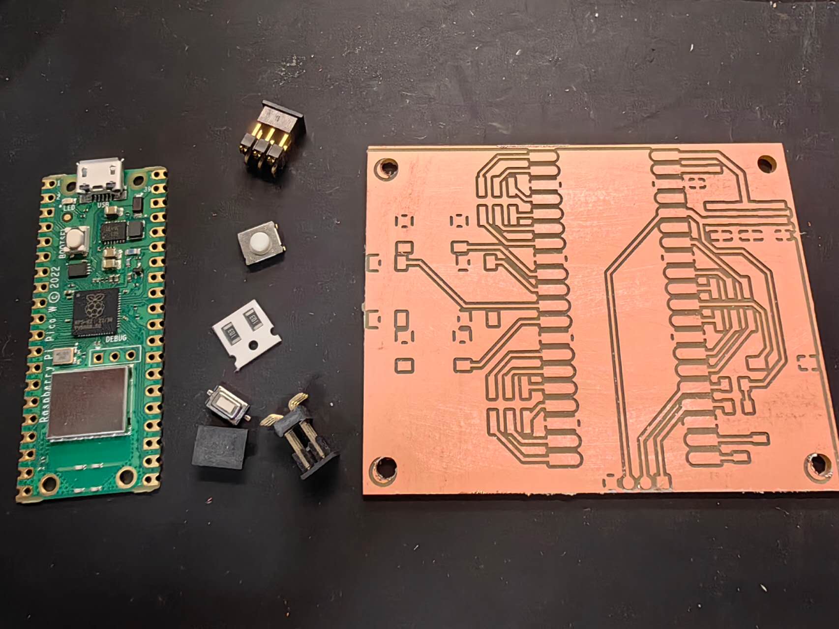
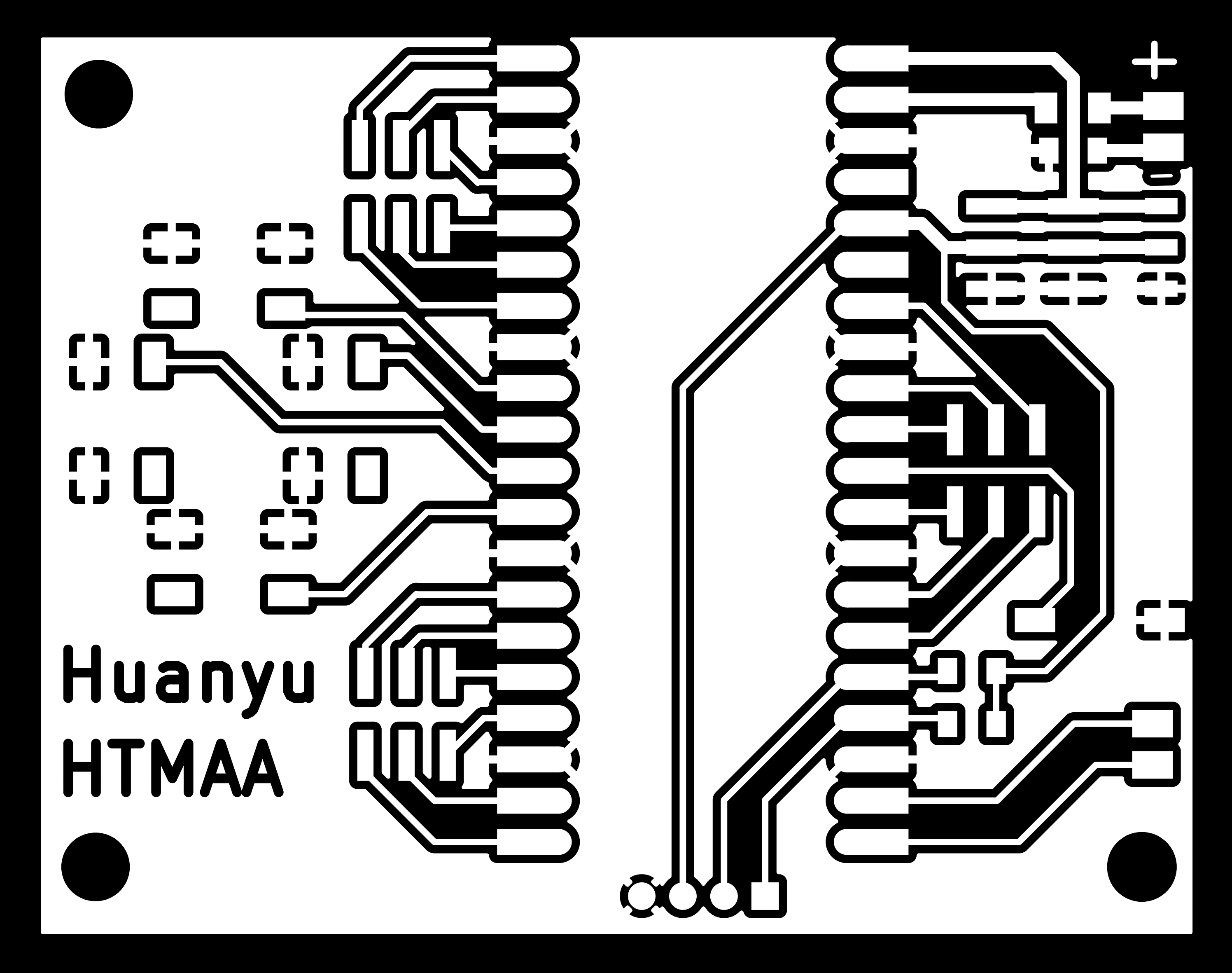
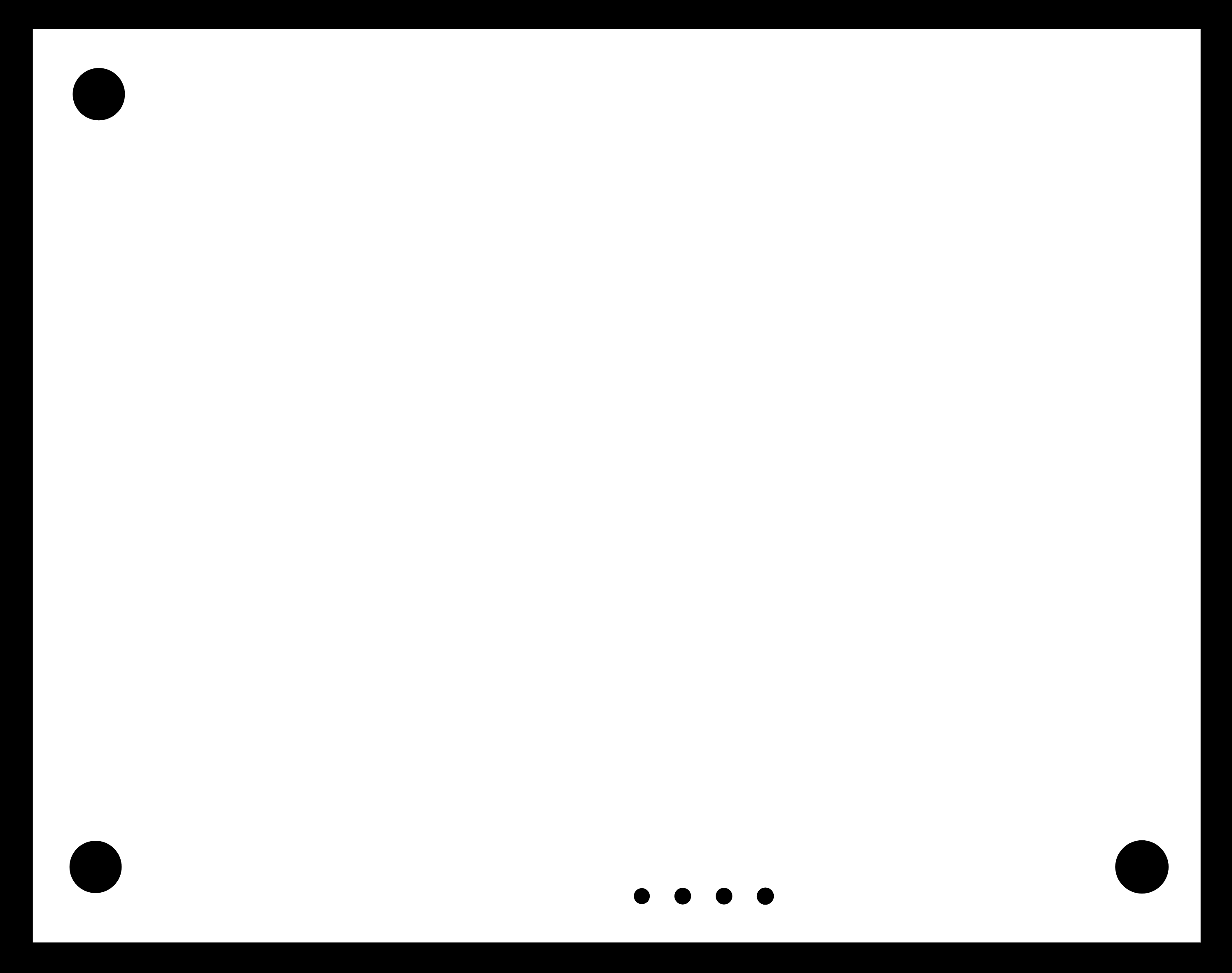
To solve the problems I mentioned above, I revised the electronic designs in the shop, and now I know which electronic components we have. The design and input files look like this: 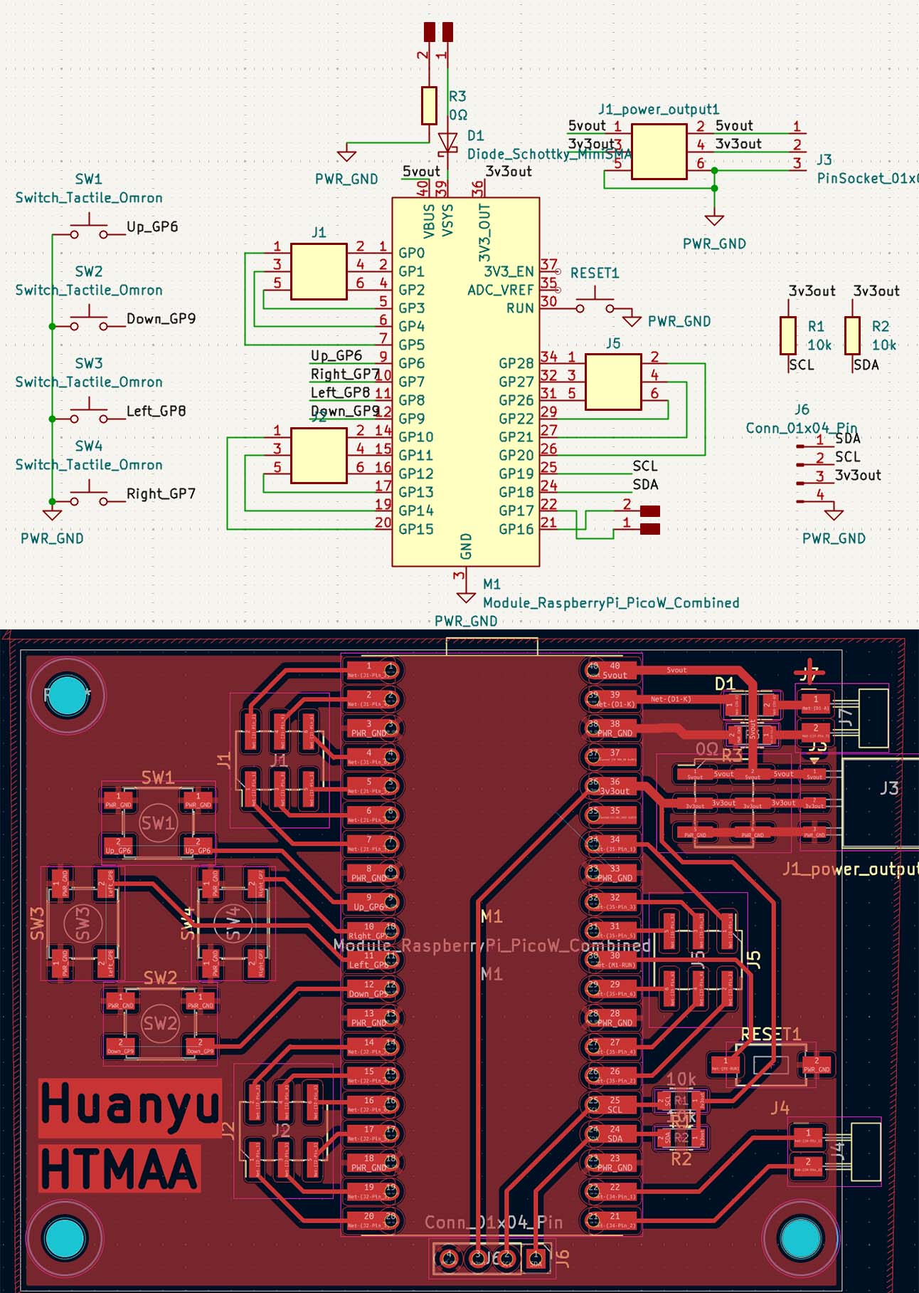
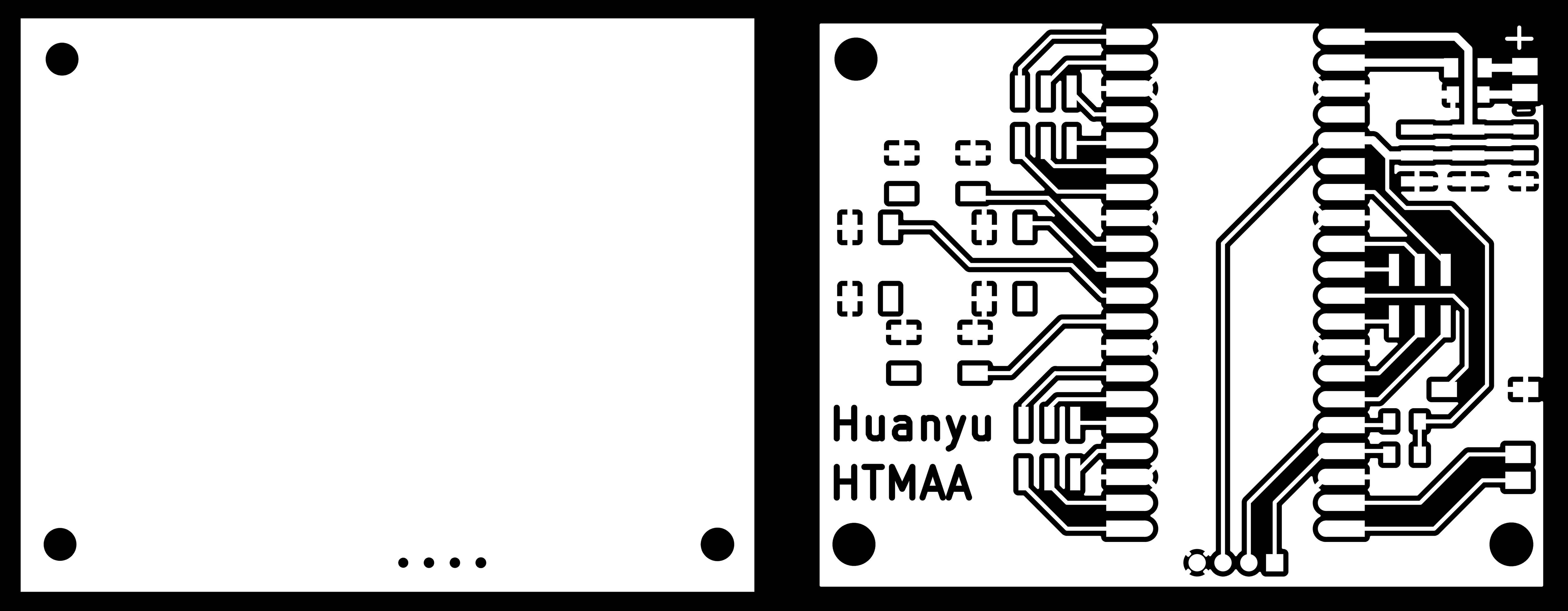
(Download: Final PCB trace PNG)
(Download: Final PCB edge PNG)
(Download: Final PCB KiCAD original design files)
I also added the additional texts on the board, and I need to adjust the size of it several times, otherwise it can’t be milled with enough resolution with the bigger end drill. Here is one of the examples of too small text size: 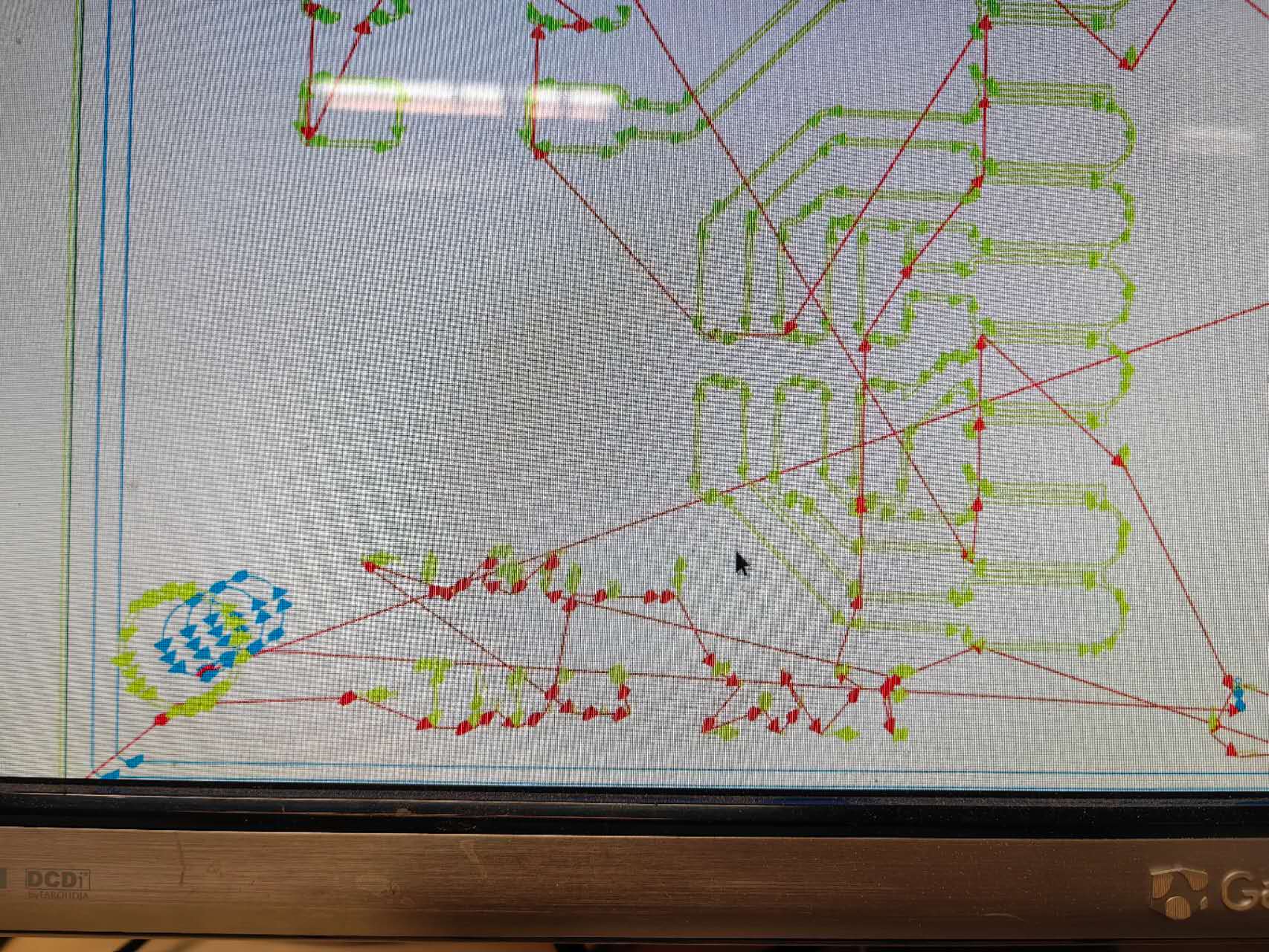
After a long soldering experiment, the finished board looks like this:
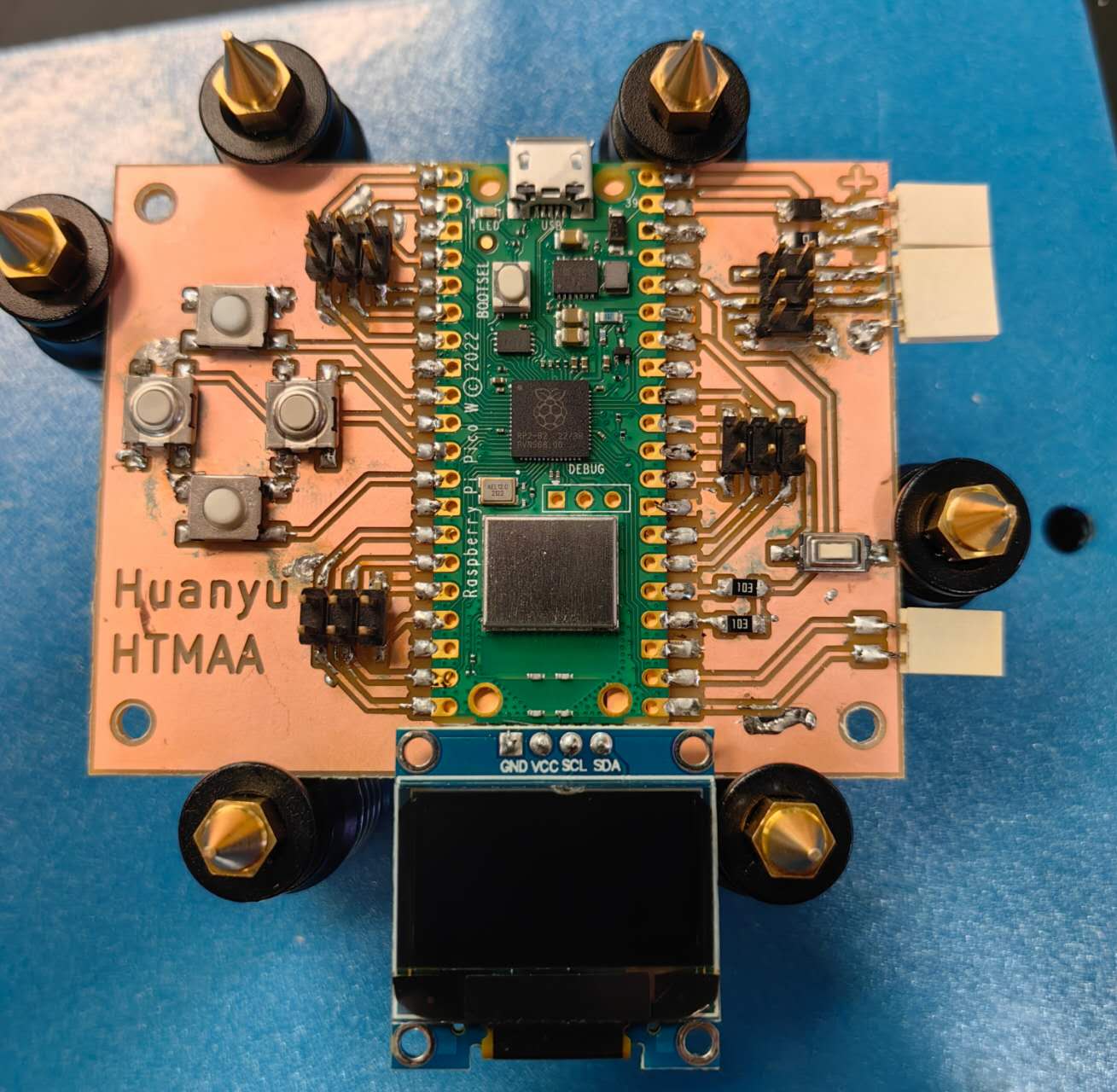
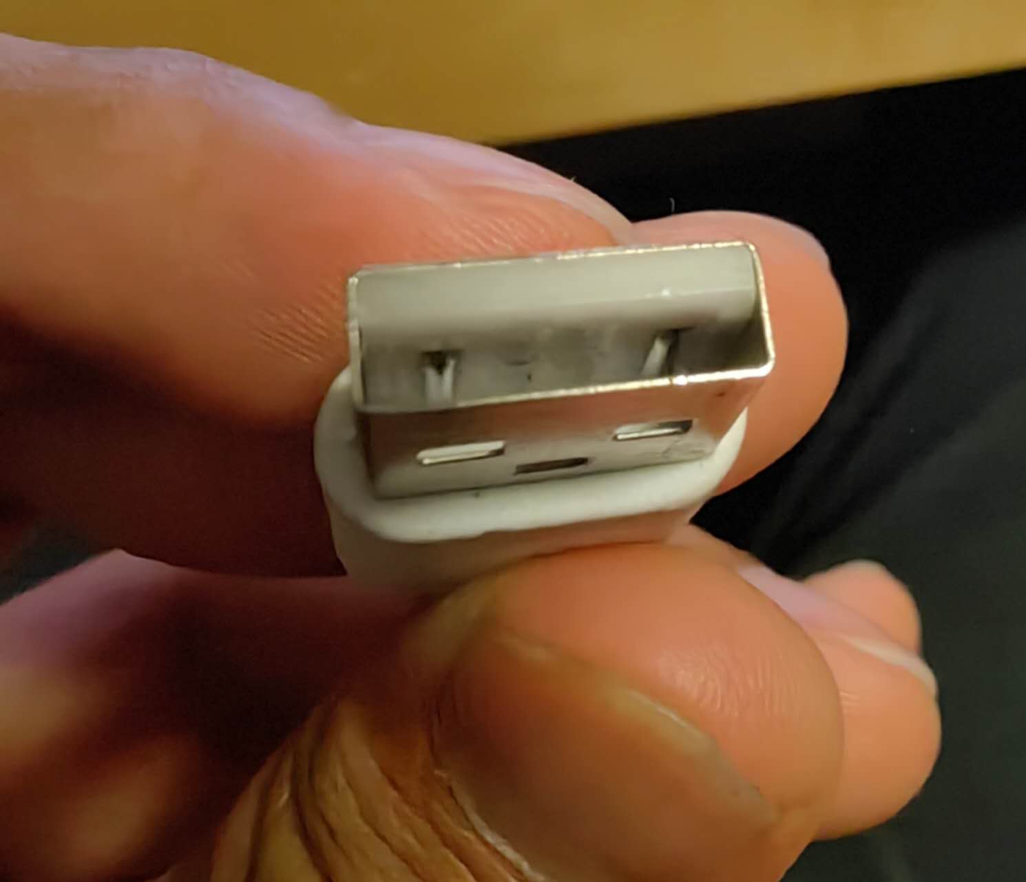
Sadly, I didn’t get a chance to upload the test codes for it because I figured out the only mini-USB cable I have is only for charging. If we look inside the port, there are missing connectors for the information transmission.