Assignment
group assignment:
 • use the test equipment in your lab to observe the operation
    of an embedded microcontroller
individual assignment:
 • use an EDA tool to design an embedded microcontroller system
    using parts from the inventory,
    check its design rules for fabrication,
    and simulate its operation
 • extra credit: try another design workflow
 • extra credit: design a case
Electronics Design
I was looking forward to this week quite a bit, but it ended up being very frustrating. Many thanks for Quentin and Ceci for helping me with some of my questions!
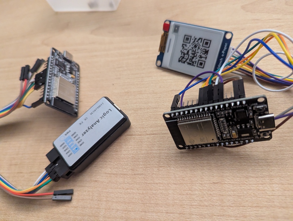
It started well. I received my $12 logic analyzer in the mail and spent part of that evening analyzing the SPI connection between my ESP32 dev board and the e-ink display. I have 2 of these dev board so I put the same code on the second one in order to not fiddle too much with connections while swapping display and logic analyzer (my probes haven’t come in the mail, yet).
First, I installed PulseView but making it set up the driver for the logic analyzer didn’t work as expected. It kept saying that it can’t find the logic analyzer. A review on Amazon put me on the right track and I used Saleae’s Logic 2 for the setup. To quote the amazon review (from the product link above):
Configuring it to function with Sigrok’s PulseView and Saleae’s LOGIC proved just a small ignorance-induced challenge on a Windows 10 x64 newly build workstation, but I was able to get it installed and functioning as intended/desired. It ended up being a pretty shallow learning curve I needed to progress through. Youtube videos and Amazon reviews & buyer question responses helped. User tip: Use Saleae’s LOGIC to get the newly connected device configured with drivers, once that is done, try Sigrok’s PulseView, prior to trying to force a square peg into a round hole with their Zadiag tool…
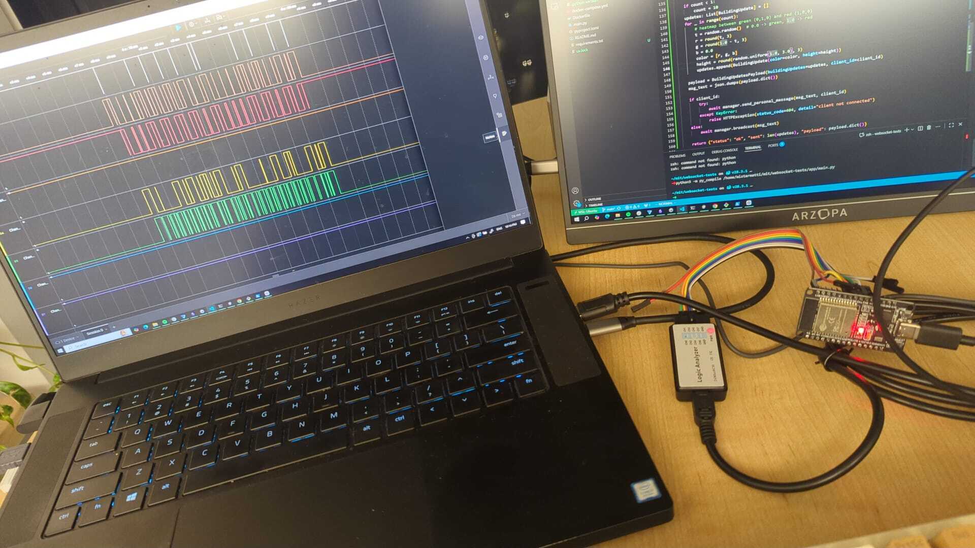
Once correctly set up, I was able to run the code on the ESP32 dev board and get data into Logic 2. I initially didn’t quite understand what I was looking at. I knew the byte sequence that the ESP32 sends across the connection but the logic analyzer showed me a different byte sequence.
My problem was that I didn’t set the “enable” channel for the SPI connection in Logic 2. I didn’t realize that “Enable” and “CS” are the same thing and had just ignored it. When I set the “enable” channel to the DC output of the ESP32 the control bytes that the ESP32 sends to the display showed up correctly. Success!
Tool Sessions
To learn more about debugging tools, we met in the electronics workshop at the Media Lab. Ben, Ceci, Eitan, Tyler and I participated - with Ben and Ceci having the most experience of the group and essentially teaching the rest. Eitan took great notes which he published here.
I had experience with voltmeters before and had just started playing with my new logic analyzer the night before. I hadn’t used an oscilloscope or a bench power supply before.
The session Ben and Ceci led was great and I also joined the TAs the following day. The topics covered were essentially the same, but I was able to ask some more questions about logic analyzers.
Design
I realize in hindsight that I’ve set myself quite a challenge for this week. I’m generally not unhappy with what I’ve learned, but I think this wasn’t the cleanest way to do the assignment. I will even accept that I failed part of the assignment (the simulation).
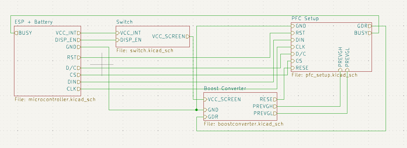
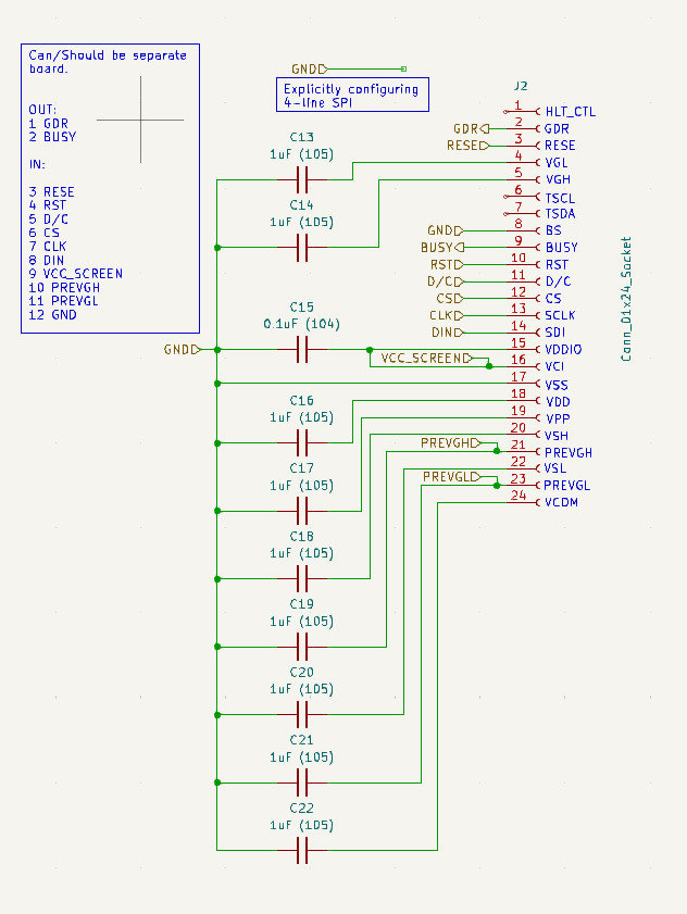
My goal for this week was to replace the driver board that the e-ink display comes with so that I can use the display itself and plug it right into a custom board. The driver board comes with a schematics pdf, and the display itself has a data sheet that also has a reference implementation.
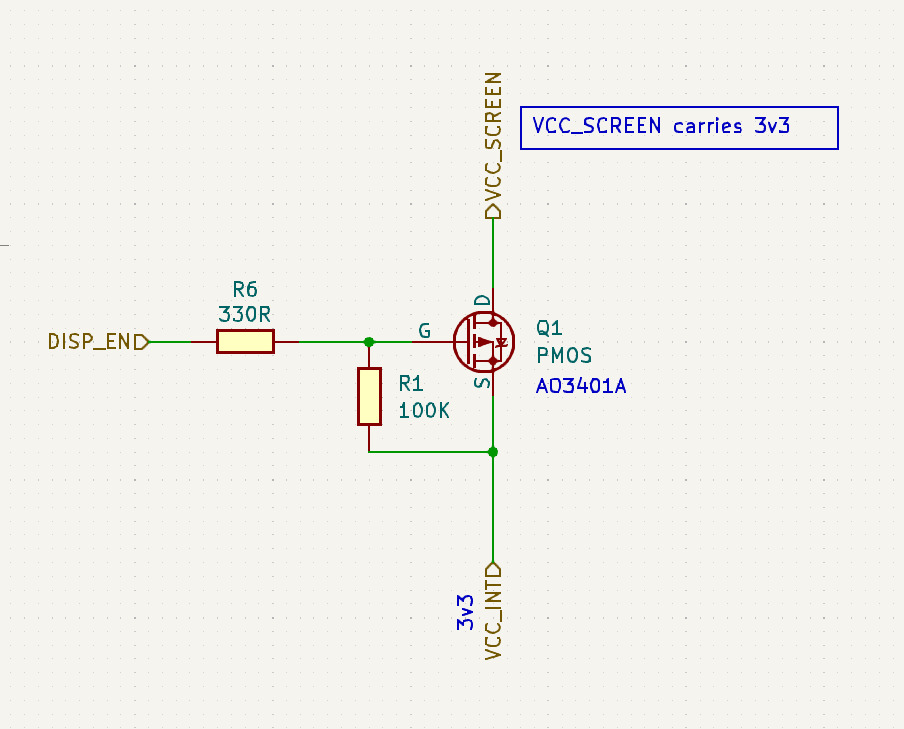
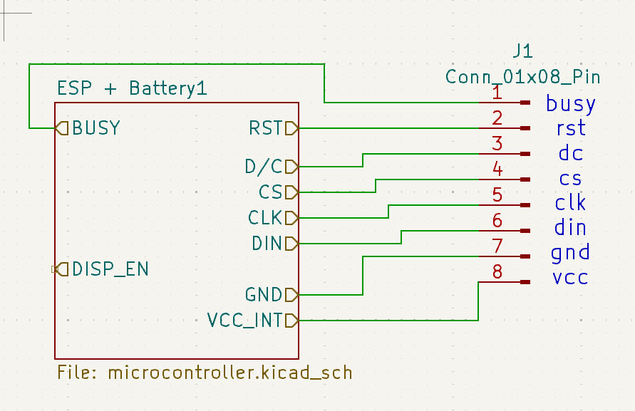
I intended to throw out all the components that aren’t needed as I’ll never run my custom board with a 5V microcontroller and the original schematics include a lot of level shifting. I created hierarchical sheets in KiCad to separate the individual components (Battery + ESP32, switch, boost converter and connector setup). This seemed like a good idea considering that there the connector for the display has very thin pins and I won’t be able to mill the respective footprint on the regular milling machine next week. When talking to Quentin he suggested that I could make a breakout board on the laser in his lab. So, having the connector design separately seemed like a good idea. This came in handy later on as we will see.
Simulation
I highly doubt you’ll be able to simulate that
- Quentin
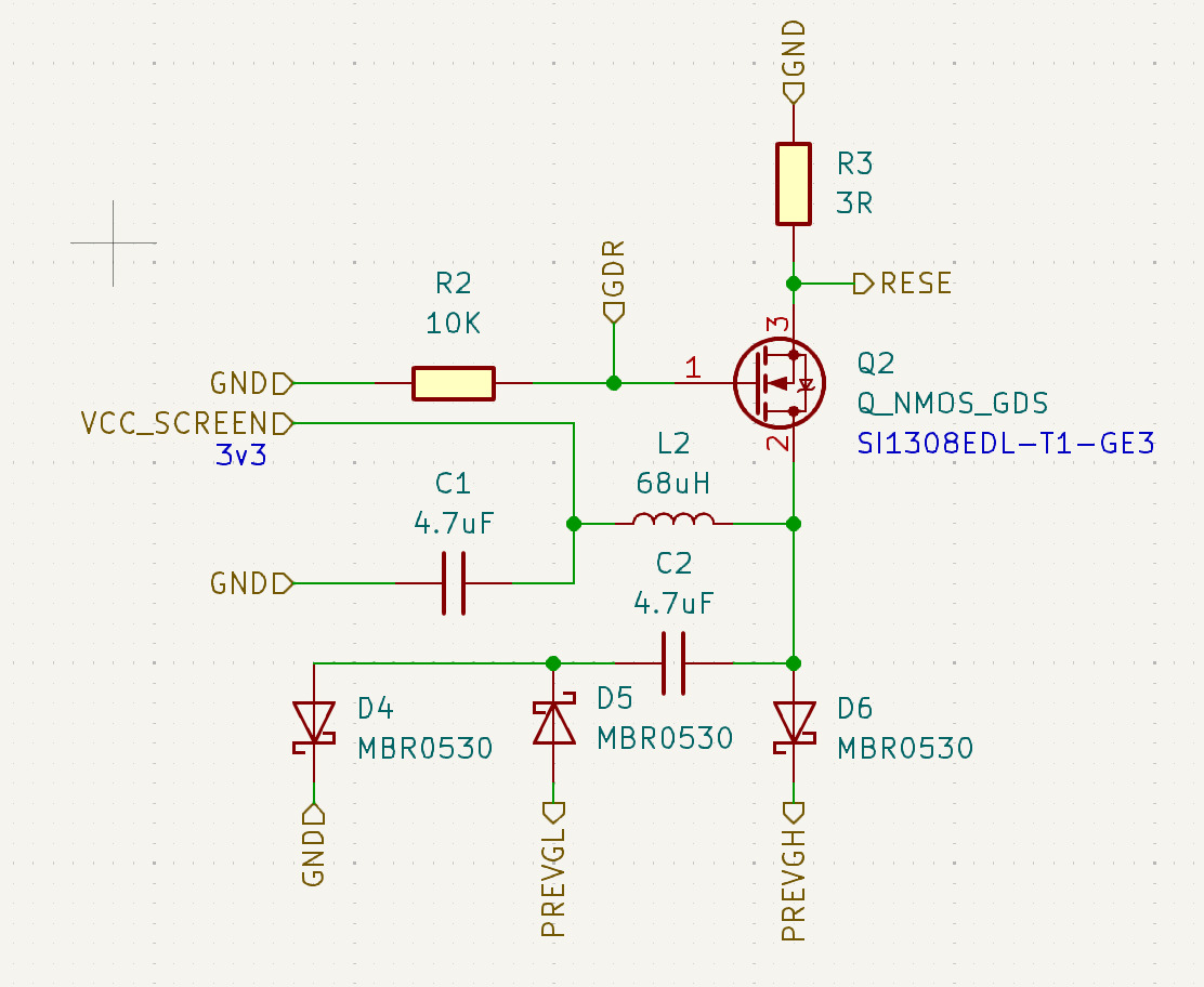
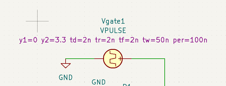
I have never made a boost converter before. That’s why I was keen on trying to use KiCad to simulate its behaviour. To have a chance to simulate it, I pulled out the boost converter components into a new KiCad project. The gate of the mosfet in the boost converter is driven by an output pin on the e-ink display. It is able to drive up the voltage to up to 20V which is what’s required to refresh the display. To be able to simulate the design, I added a square wave with an initial duty cycle of 50% to mock the output of the display (the respective pin on the display is called GDR).
Unfortunately, I didn’t get anywhere with the simulation part of it. I ran into many issues that I didn’t understand. I also talked to Ceci and we couldn’t quite make it work even though she had some experience with a different simulation tool (ltspice, KiCad uses ngspice internally). Unfortunately, this meant that I spent many hours without much to show for it. That’s ok and I’ve learned things in the process, but it wasn’t helping towards the goal of getting a board designed and simulated. In the end, it cut so much into my time of actual board design that I had to simplify what I was going for this week. Ultimately, that might have been a good decision anyway. The original board design had, like I said, a component on it that uses very small pins. This component by itself, violates the design constraints imposed by the in-house manufacturing process.
I’m adding the simulation test file I set up to the list of files on the right.
Learnings
- Simulation is difficult and not as easy as I thought
- A lot of the simulation models in KiCad seem to be for “ideal” components. I found advice online to add small resistors in series with these components to mimic their resistance.
- KiCad doesn’t seem to be able to simulate parts of the circuit in isolation which is why I broke out my boost converter schematic into a new project.
- Simulating this sort of board where part of the signal is unknown (GDR) is tricky. I had hoped I could mock the signal and figure out what it would have to look like with the simulation.
- It seems like for this sort of work, there are rules of thumb in terms of what components to use - and most people then just build and don’t worry about blowing up the occasional capacitor.
Board For Next Week
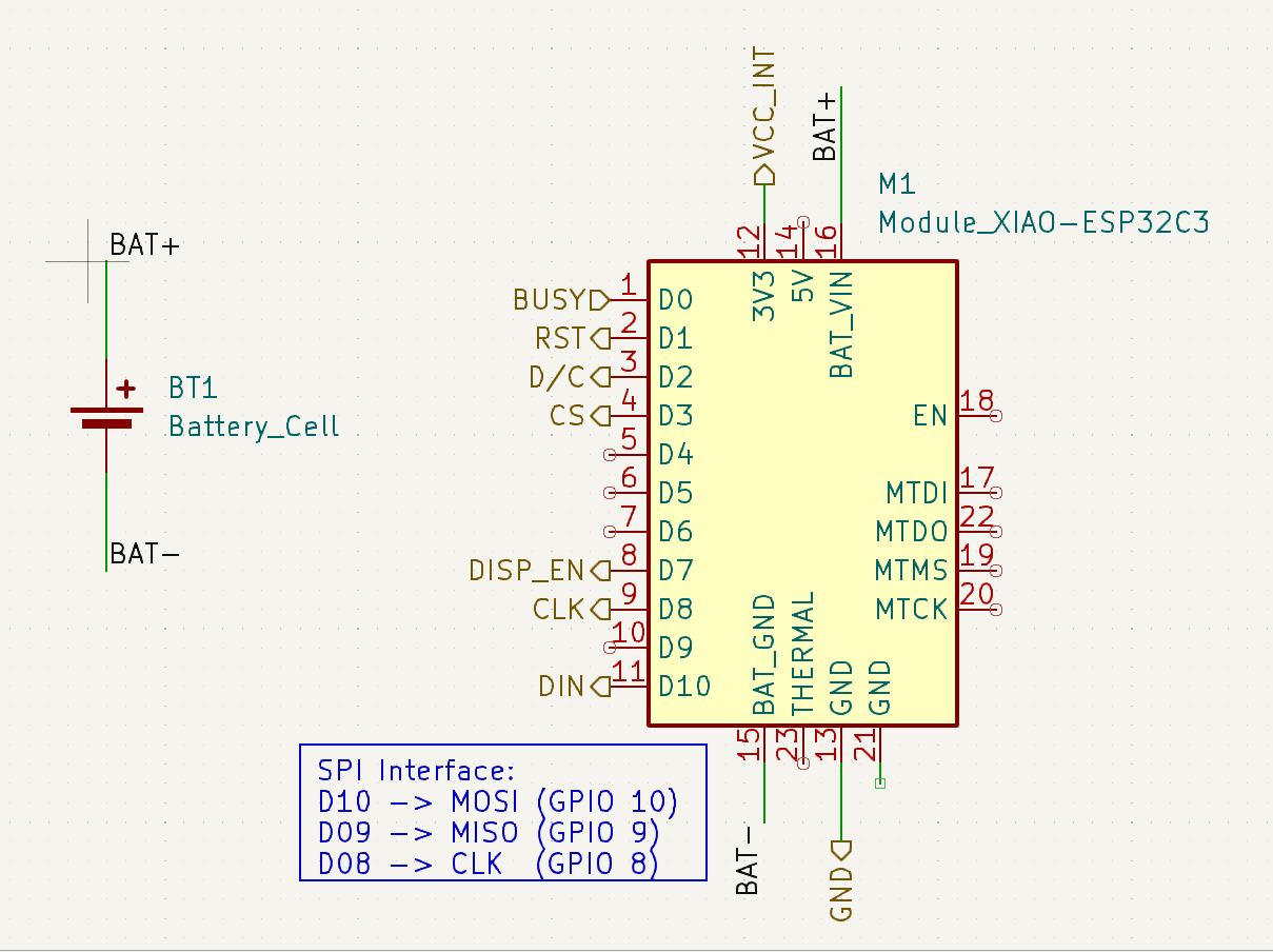
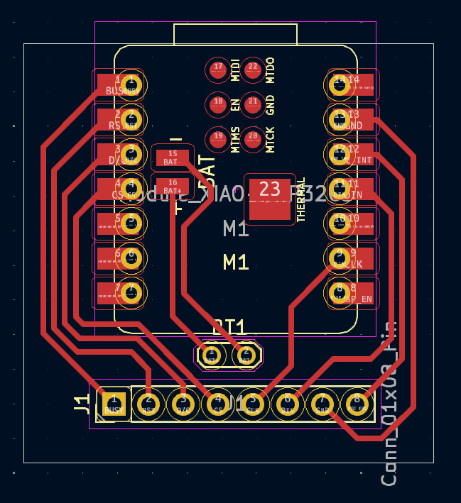
So, to have something to show and to be able to manufacture something next week, I made a simpler design that connects a battery to the Xiao and also breaks out the pins in the right order such that it’ll be easy for me to solder on wires that connect to the display. This final result is a few steps below what I have hoped for as a result of this week’s efforts, but considering that Electronics Production week is coming up, I’m ok with having something that I can make. My DigiKey order containing the PFC connector has not arrived yet anyway, so I would’ve been limited in my abilities to make a more complicated board next week no matter what.
I am hoping that in this coming week I can still make some progress on the design that brings a lot of the required components off of the official driver board and onto a custom board.