Assignment
group assignment:
• characterize the design rules for your in-house PCB production process
• submit a PCB design to a board house
individual assignment:
• make and test an embedded microcontroller system that you designed
• extra credit: make it with another process
Group Assignment
The documentation for the group assignment can be found here. We learned how to use the Carvera milling machine (thank you Quentin!!) and then also worked together as a group to go through the steps of submitting a board design to JLCPCB.
Individual Assignment
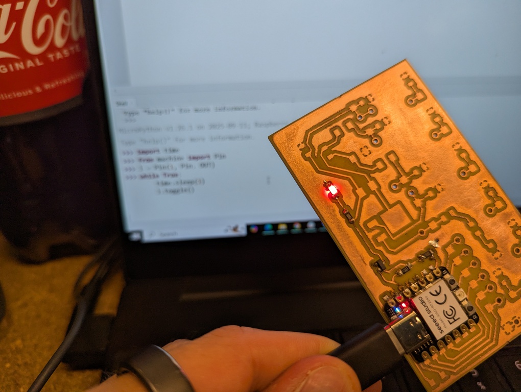
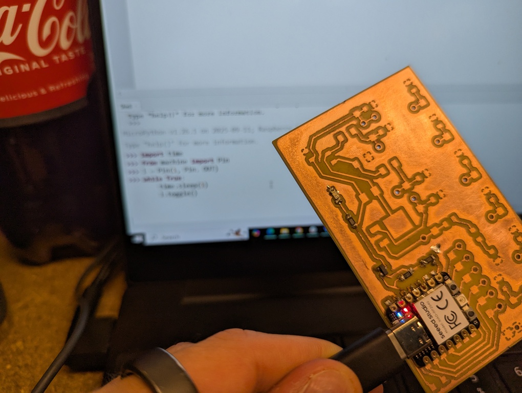
I’m continuing last week’s work. As a reminder, I’m trying to re-make a driver board for a Waveshare e-ink display. As a simple first step, I’m aiming to have an LED blink on a custom board so that I fulfill this week’s assignment. I’ve added the respective LED into my design. I placed it on a line that is controlled by a pin on the microcontroller that is supposed to control whether the e-ink display gets any power or is switched off. This switch is implemented through a p-channel mosfet. To switch it on, you pull the pin LOW.
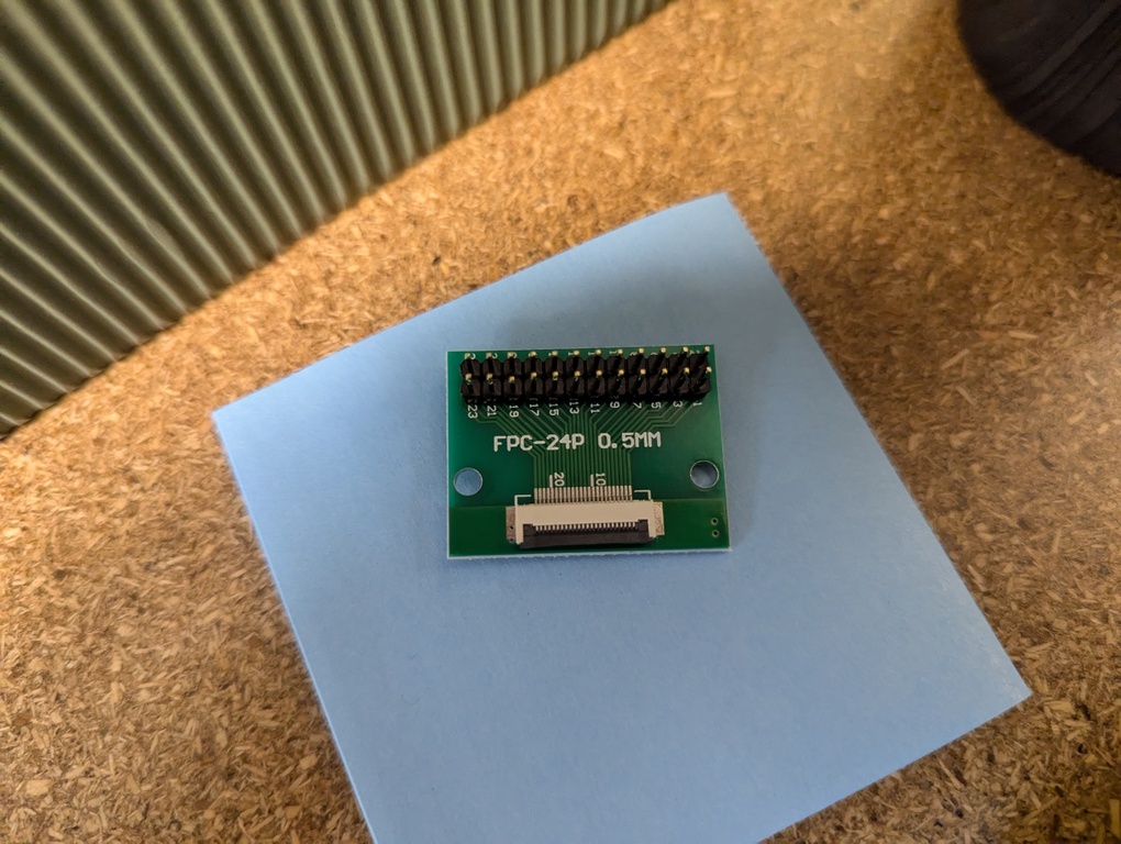
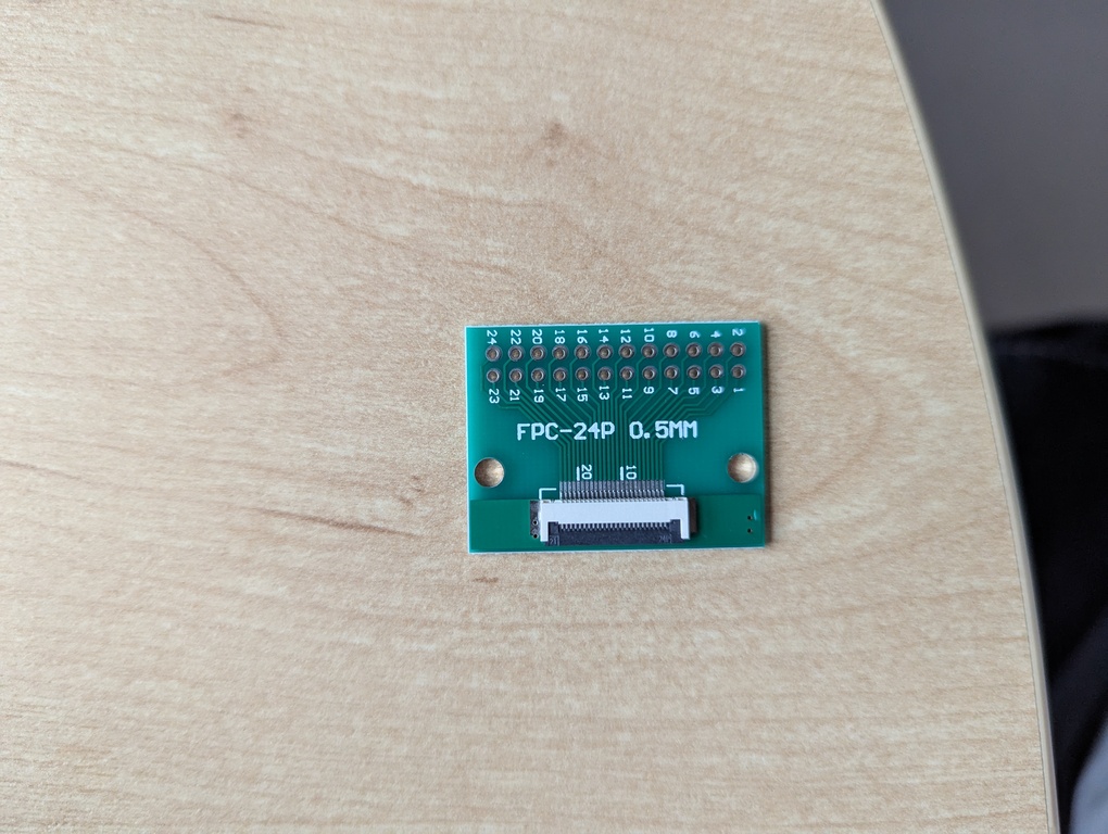
My design is a little convoluted and I can clean it up quite a bit. I call it convoluted because I still have last week’s hierarchical schematics in my KiCad file, and I’ve set things up in a way that allows me to test my design with a commercial breakout board that I bought, as well as with a custom breakout board that I was hoping to make with the high-precision laser. Spoiler alert: The FPC connectors that I ordered from DigiKey didn’t arrive in time so I had to stick to the commercial board as shown below.
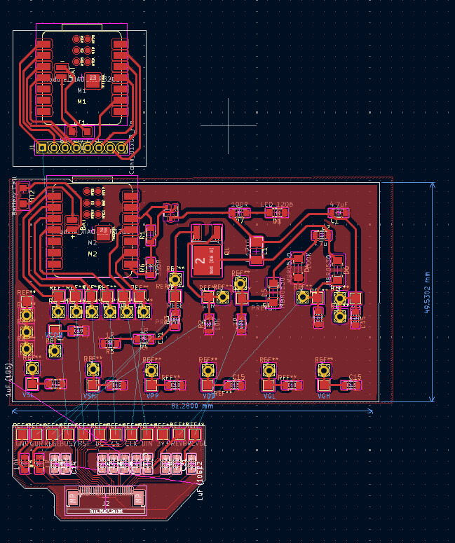
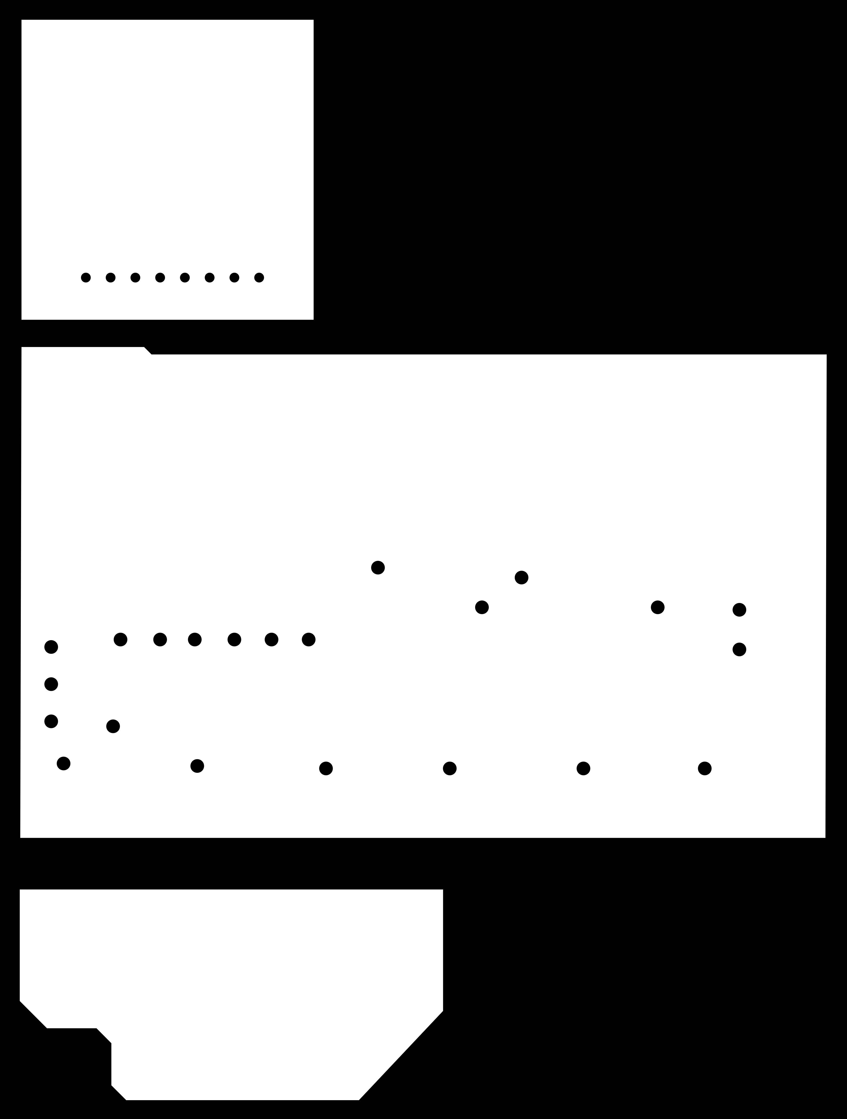
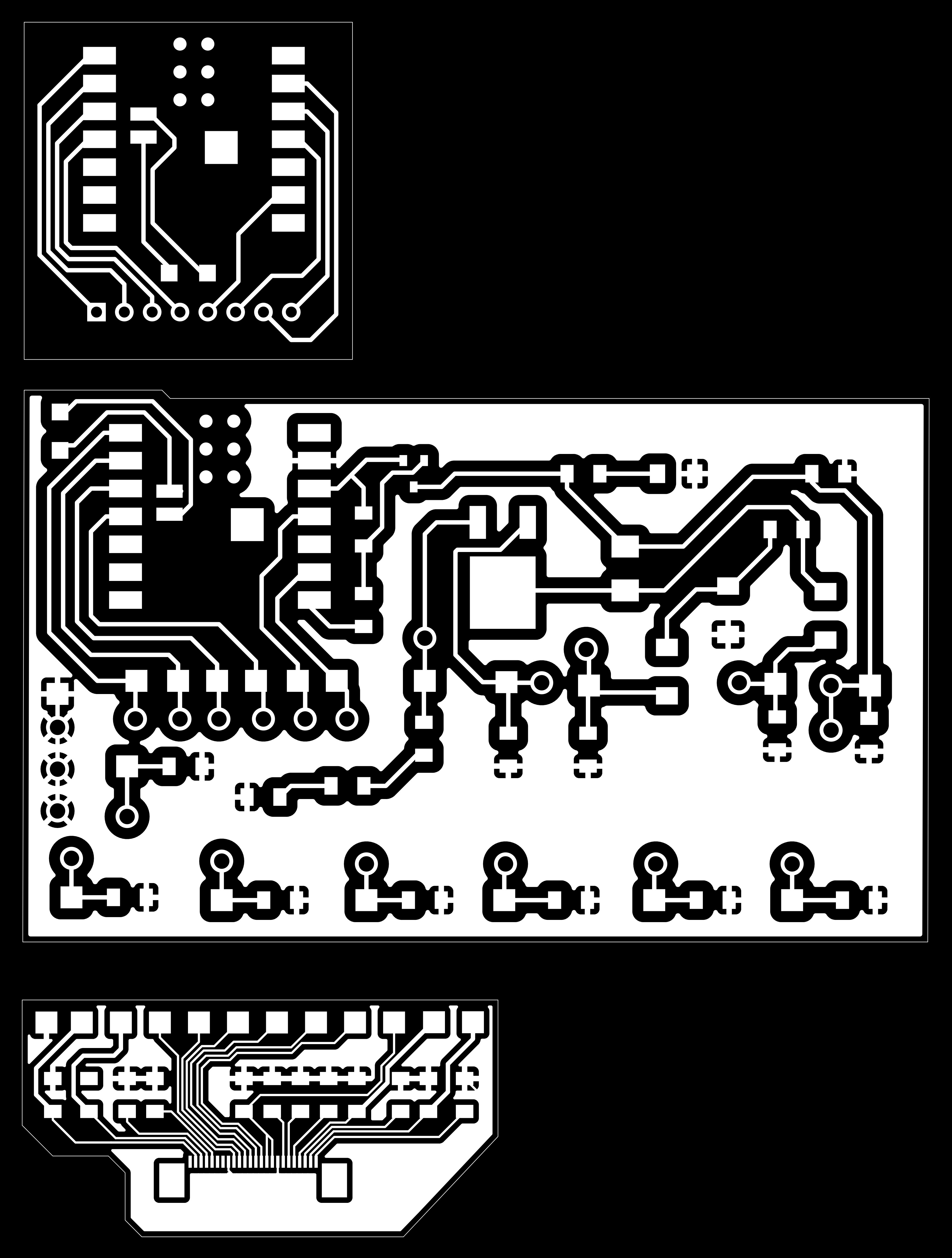
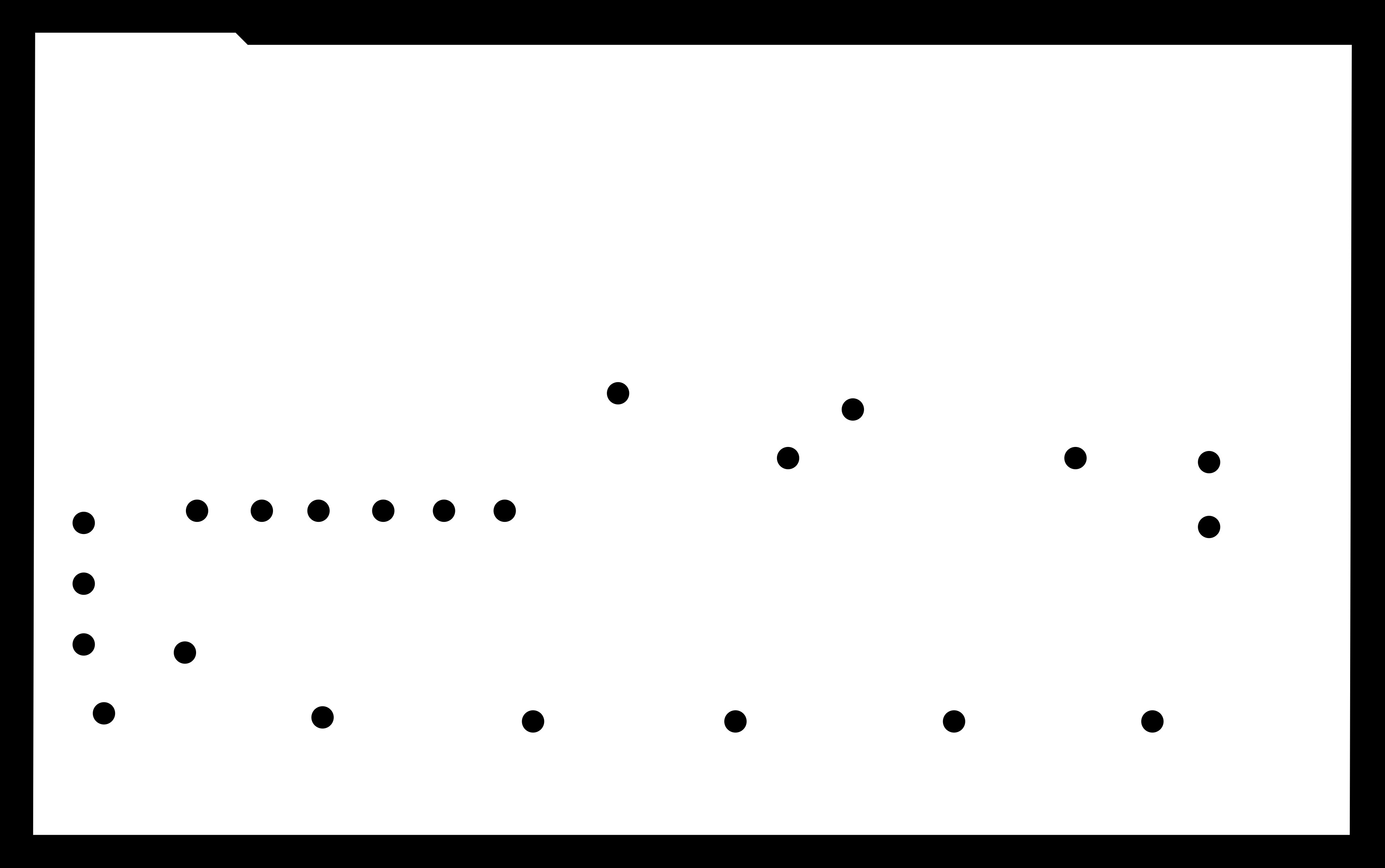
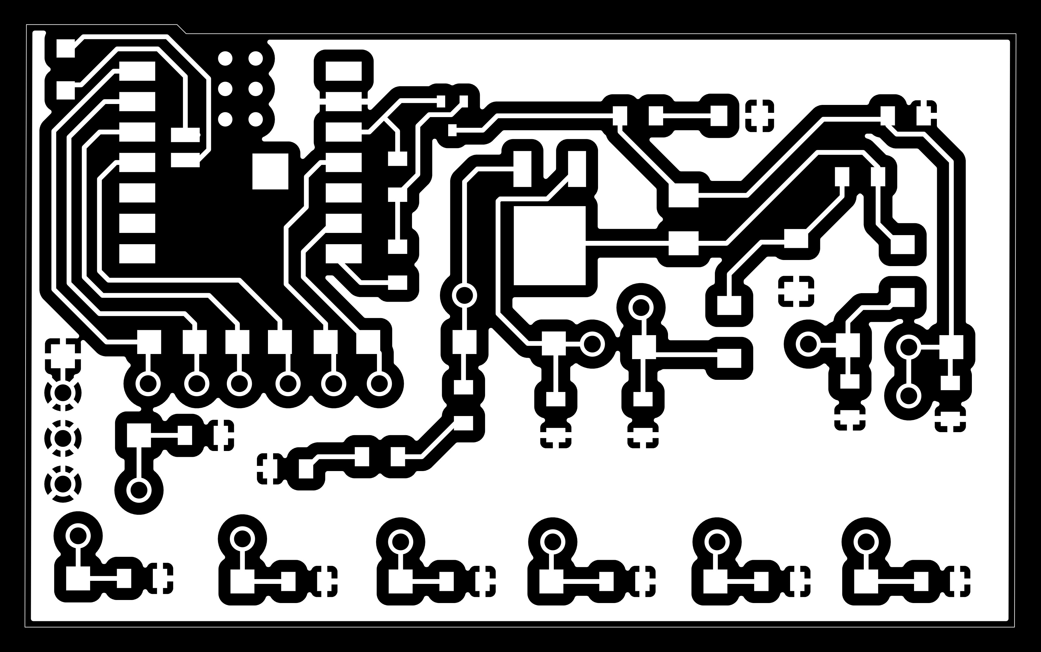
As shown in the image, I have multiple boards in my KiCad file. Since the Carvera milling process that we use is based on images, which get processed into gcode, I am able to use this sort of setup without too many problems. I exported the gerber files from KiCad and processed them into the images shown below that show all 3 boards. Using Gimp I then cropped out the board I wanted to make and discarded the ones that I wasn’t ready for and didn’t want to make. The process is simple, but I found that it’s easiest to
- open both files in Gimp
- drag the image layer from one file into the other
- verify that they’re aligned correctly by switching the top layer on and off
- apply the crop
- export the images one after the other by toggling off the top layer

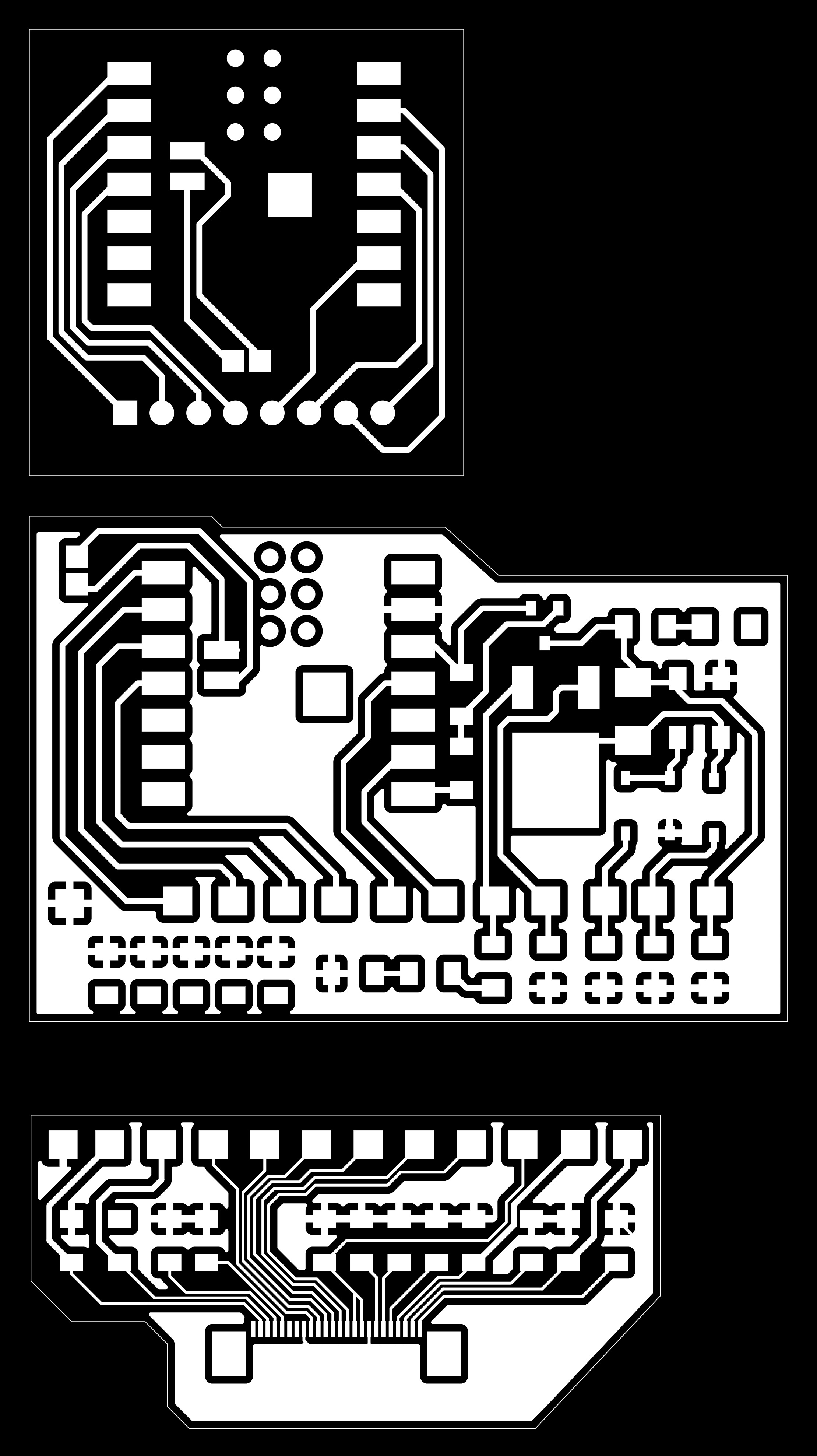
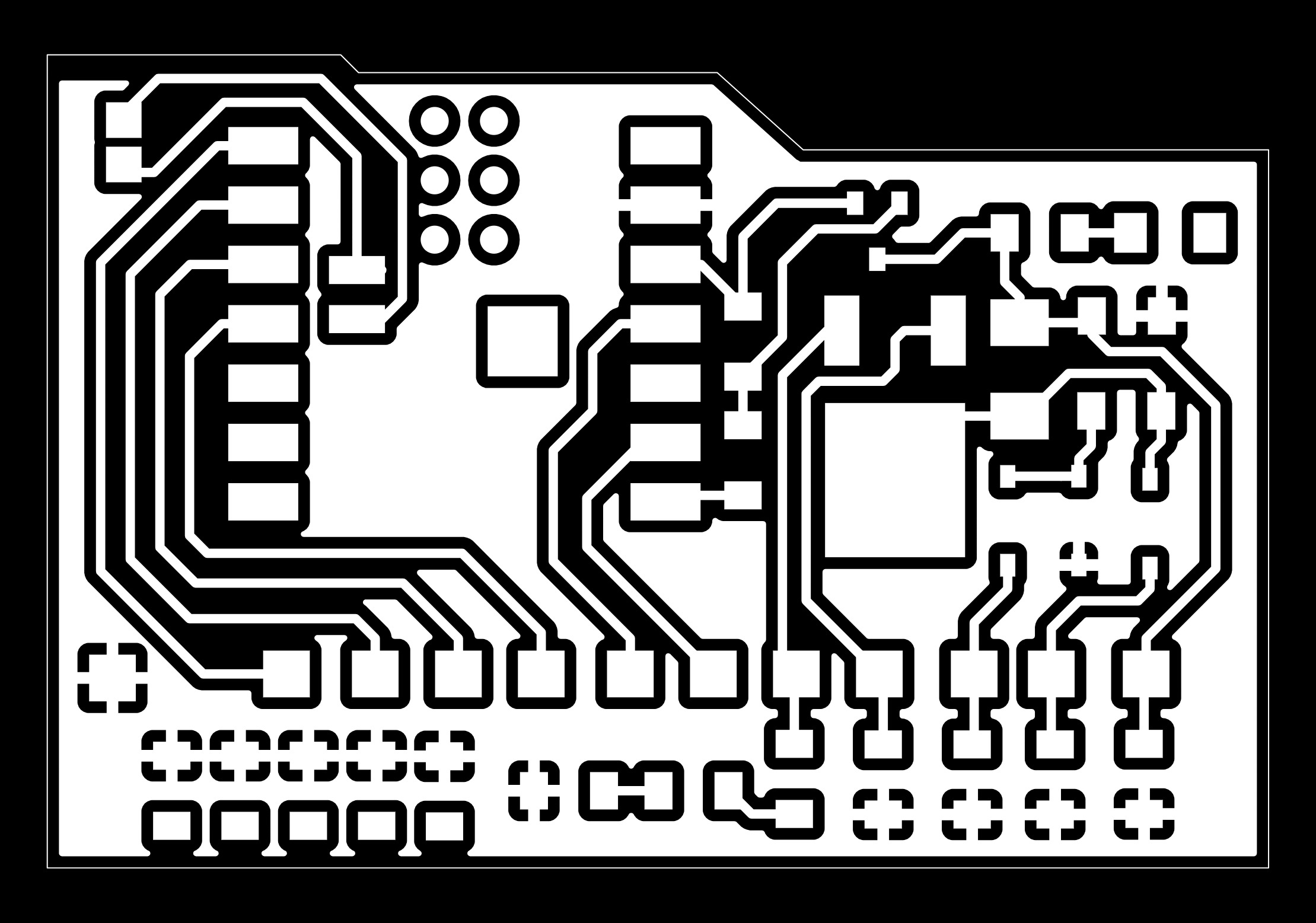
Using Neil’s mods toolchain, I converted the images into gcode and made a board on the Carvera machine.
Using my board, I was able to assemble the sub-circuit that drives the LED. I ran into a few problems.
Missing Connection To Ground
I noticed that the LED’s cathode (which needs to be connected to GND) landed on a pad that had no connections to the ground plane. The problem was a result of my hacky multi-board KiCad setup. That particular pad had a connection to a GND net that wasn’t the one I used for the other pads and the ground plane on this particular board. Hence, there was no connection and I had to make a manual bridge with a blob of solder. Worked fine, but was an oversight on my part in the design stage that could have been avoided. You can see how I fixed the problem in the above image.
Mosfet Heating Up
I also had a problem initially with the mosfet heating up a lot. The culprit was a short caused by a bit of solder that connected one of the resistors to ground. It also prevented the LED from lighting up initially. Luckily, the short didn’t cause any other problems and I caught it relatively quickly. It was resolved quickly with a bit of desoldering wick.
Custom Footprint
I had made/modified 2 footprints for this board. For the Xiao footprint, I removed all the holes which was easy enough and successful. I also added a custom footprint that was intended to allow me to connect a battery to the board. I didn’t get around to testing the battery this week, but when I first made the board I noticed that the 2 pads I added to the footprint weren’t separated correctly. Clearly, I didn’t add enough clearance between the pads. Separating them with a box cutter was easy enough, though.
Moving on
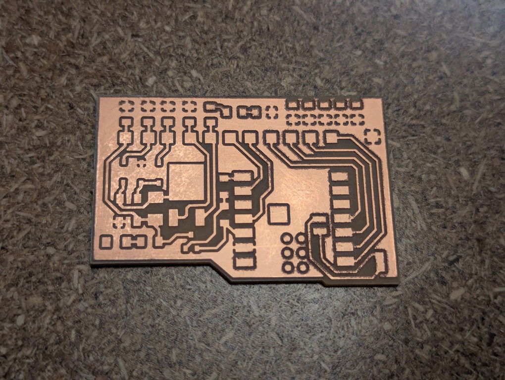
I then proceeded to soldering all additional components onto the board - I tried at least. I was a little too optimistic in my design and overestimated my ability to solder small components that are placed very close to each other. I used the minimum clearance of 0.4mm for all traces as well which caused some additional struggling. To top it all off, I noticed that the footprints I used for the 3 diodes in my design were sub-optimal. The pads were very small and the diodes large enough to touch the ground plane surrounding the diode pads when soldered on. I tried to manually add more clearance to those pads by scratching copper off of the ground plane, but it didn’t work very well. I actually messed up my board quite a bit in the process. Copper traces came off, when trying to solder to the diode pads and some parts of the board ended up quite charred.
It was time to make another board.
I took my learnings into the re-design:
- ADD MORE CLEARANCE.
- Improve the diode footprints by increasing the pads.
- Space out all components much more to make soldering easier.
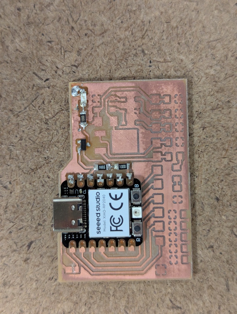
I fixed the problem with the missing ground plane connection as well, and after fabrication soldered the LED sub-circuit onto the board. The below images show the blinking LED.
I then proceeded to solder all remaining components onto the board which worked much better this time. The larger clearance between traces and ground plane helped a lot, and I had gotten better at soldering, as well. I was quite happy with how the soldering went on this new board. During the re-design stages I had also added additional pads and holes for headers so I could try to connect the board to the commercial breakout board I bought for connecting to the e-ink display.
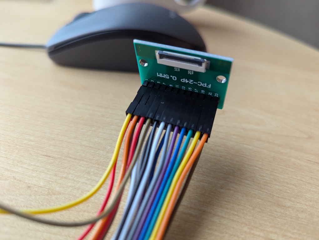
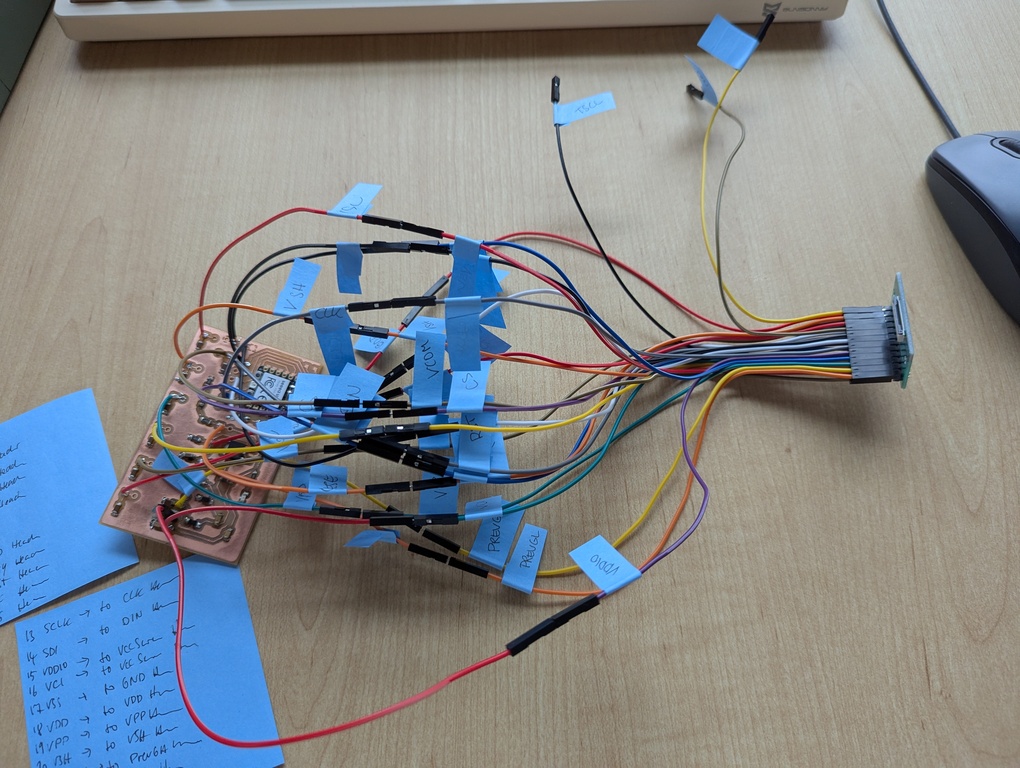
For the breakout board itself, I soldered on the headers and then attached a bunch of wires. In hindsight, I should have added a clean header to my custom board as well, to make connecting the two easier. I opted to not add that header because it would have made routing the traces on the board MUCH harder. I would’ve had to design a 2-sided board (or use many 0 ohm resistors to jump across traces) and naively I assumed that soldering on some additional wires and connecting the boards that way would be easier. I don’t think it was easier that way. You live and learn. You can see the mess of wires that I ended up with below. I very diligently labeled all wires and made sure the colors line up, and while I think that made the process better overall, it was still quite the mess.
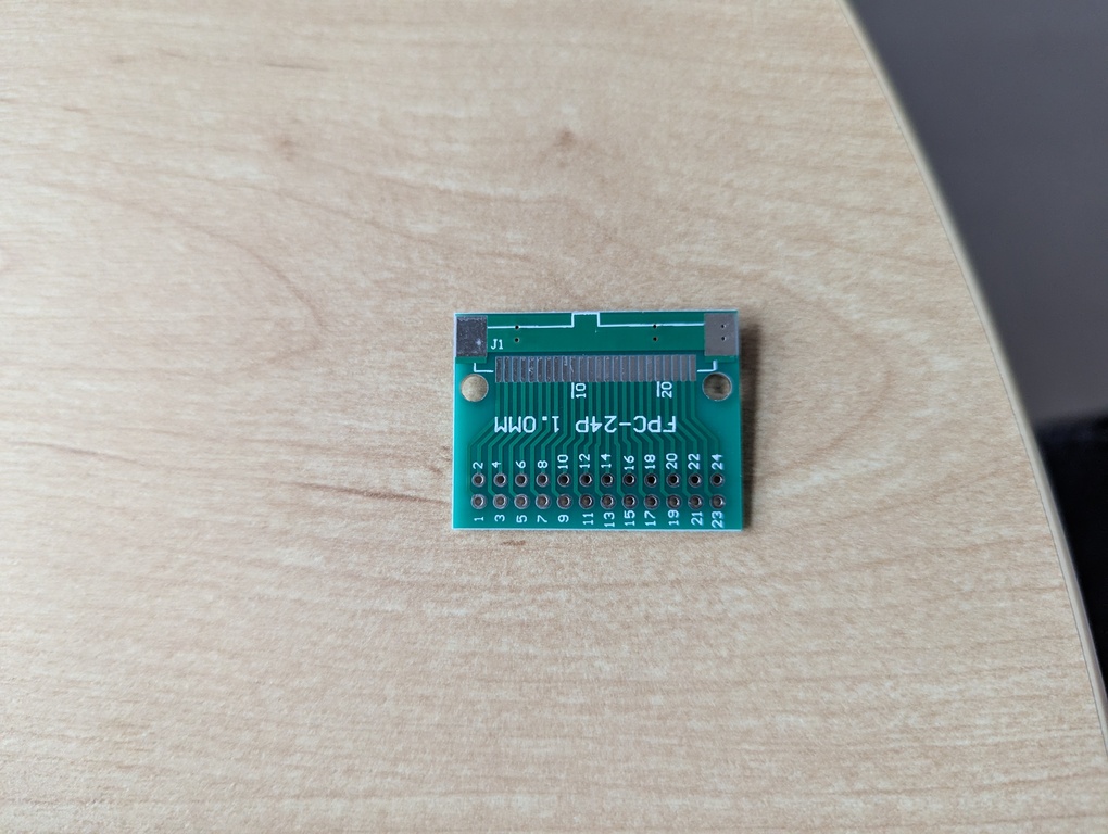
I want to also call out a “problem” I noticed on that breakout board I bought. When I did continuity tests with the volt meter, I used the bottom side of the board because it has exposed pads there. Note in the images that the labeling of the holes is NOT consistent between the top and the bottom. I had a brief chat with Ceci about it and we concluded that they probably use the board for FPC connectors of different widths (wider connector on the bottom side) and that they don’t expect the user to correlate the pads on the bottom to those on the top. The bottom and top should be thought of as 2 separate boards. I’m pointing this out because it took me a minute to understand why my continuity test wasn’t successful when I first tried it. The problem was that I was testing pad 1 instead of pad 24 because of the inverted labeling.
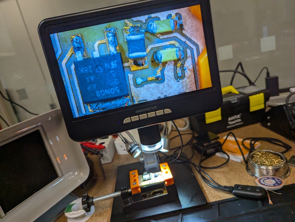
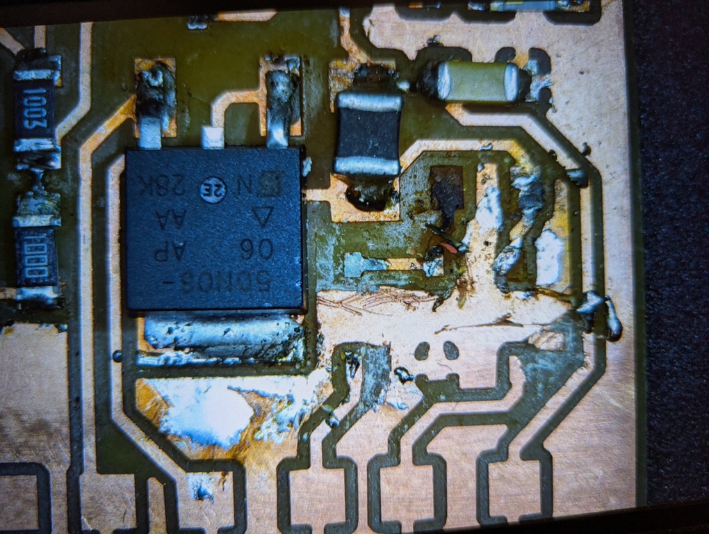
Unfortunately, my board doesn’t work as I would have expected. I’m not sure yet if it’s the boost converter that isn’t working or whether the signals from the microcontroller don’t make it into the right places. I will continue to debug the problem and report back here. There’s a chance that the components that I used for the board deviate too much from the components in the reference design. I had to adjust the values for the inductor and capacitors used because I didn’t have access to the exact components through the HTMAA inventory. The required values (68uH and 4.7uF) probably just aren’t as common. My understanding was that my replacement components (100uH and 10uF) should be ok in terms of the generated voltage, but clearly something isn’t quite right. As a first debugging step, I hooked up the 2 lines that are supposed to generate larger voltages to the oscilloscope. It was a great opportunity to learn more about how to use it and while it’s frustrating that the board doesn’t work, I’m grateful for the opportunity to learn.
In other positive news, my DigiKey order has arrived and I now have FPC connectors available. So, if I can figure out why the board doesn’t work and fix the design, I could create a unified board that directly connects to the display without the need of a breakout board. If I can’t make this board work, the Plan B for my final project is to just use the commercial driver board. I would love to avoid that, but it’s there as an option.