PCB Production
This process took me 3 whole days. It was a very folkloric experience that felt like some kind of first-person platformer video game… Picture me, a small pixelated sprite, running back and forth through a portal (the stairs) between the electronics lab in the basement of the Media Lab and the Mars lab on the ground floor. Along the way I encountered helpful NPCs (Quentin, Alfonso, Kristof, fellow HTMAAers) who told me useful information right when I needed to know it, acquired useful objects to add to my inventory (M3 screws and nuts, insulating rubber, copper tape, etc.), and performed many silly mini-games (rerouting traces, milling, sautering, desautering, etc.). I emerged Monday evening with a working prototype!
![]()
Milling
Many things that went wrong before anything went right, when I tried to mill my PCB.
Jacqueline was having issues with ragged traces on her board. Kristof came in and found that the end mill tip was entirely broken off. He showed us how to use the tool to change out the end mill. After the tip was changed, my traces came out looking beautiful!
In gerber2img, the edge cuts did not capture the holes for the through-hole connection headers I was using. In order to fix this, I talked to Quentin and learned that I had to drag and drop the drill (.drl) and edge cut files simultaneously into gerber2img, and then the holes were there.
The traces and edge cut pngs I produced were not aligned, and I only found this out when I put them into mods and calculated the job. In order to fix this I first put the edge cuts into gerber2img, and then locked the dimensions before dragging in the traces so the images would be aligned.
Though I used the recommended 0.4mm clearance for my board setup in Kicad, when I calculated the job in mods, some of my traces were too close together. Quentin explained that this was likely because the rasterization to PNG led to some imprecisions which would increase the practical tolerance necessary for non-overlapping traces. I changed my clearance to 0.45mm and rerouted my traces accordingly.
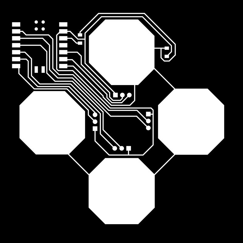
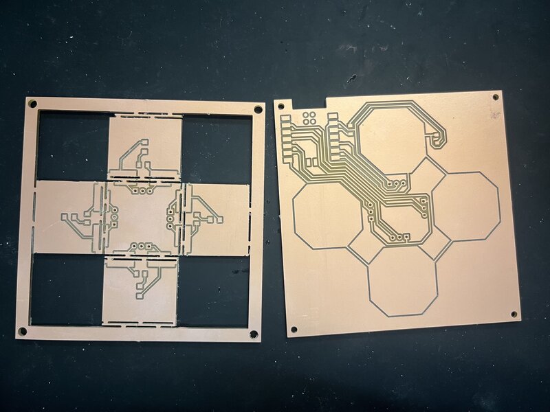
After fixing all of the above, here are the traces and edge cut pngs for my base board:
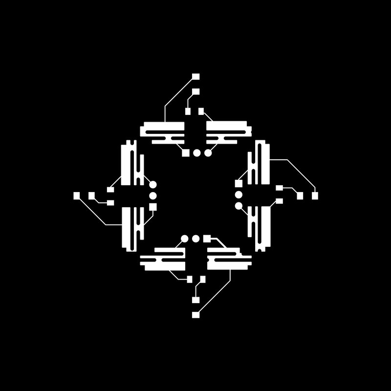
And, for my top board:
Finally, I was ready to touch the Carvera machine! More issues arose…
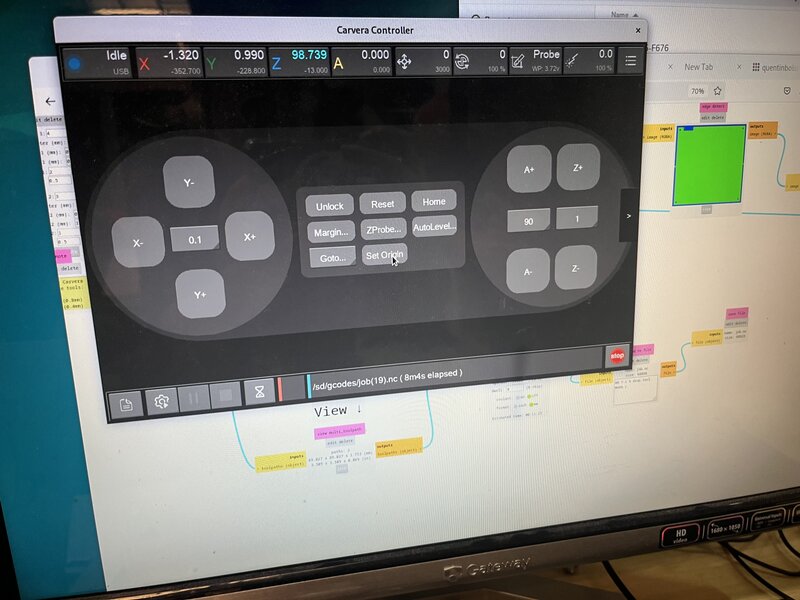
The largest single-sided PCB stock we had had holes in the corners, and the distance between the holes was just barely large enough to fit my board. I would need to be very precise with my origin calculation in order to not, for example, probe into the holes or disturb the edge of my board. Kristof showed me how to manually use the probe on the machine to interactively probe for an origin instead of using a caliper to take measurements, and this allowed us to put the laser probe right up against the edge of the hole to ensure we were getting as close as practically possible. To do this, on the Carvera interface you click the menu in the top right, select Probe as the tool on the top bar of the pop-up window, and use the X and Y controls to manually position the probe. If you try to move out of the allowable range of the mill, the “Alarm” will silently go off, and you have to unlock it in the top left corner of the main GUI window before proceeding. Once the probe is in position, click Set Origin > Set by XYZ Probe > 0 X, Y offset > OK. Here is the relevant window where the controls to set the origin with the probe appear:
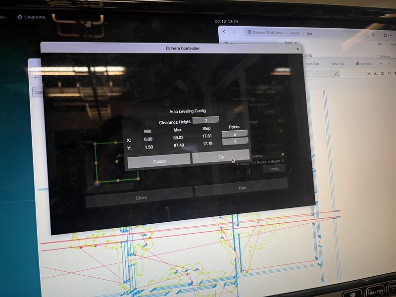
Just to make extra sure I didn’t probe into the holes, I set the automatic leveling before milling to be a grid of 25 points, and watched it the whole time with my mouse on the Stop button in case I needed to emergency stop. Here were the settings I used for auto-leveling; I also reduced the clearance to 2 so that the probe would take less time going up and down between points.
The first time I clamped in my material, it was pretty severely bowed, and I had to emergency stop it (which I luckily was able to do before any material was milled). This was due to there being burrs on the sacrificial stock I had placed underneath – sanding those off / choosing flatter sacrificial stock fixed this.
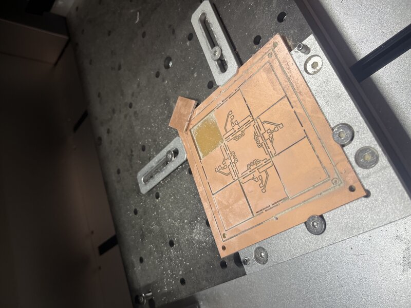
After successfully milling, here were the results of both of my boards, hot off the machine:

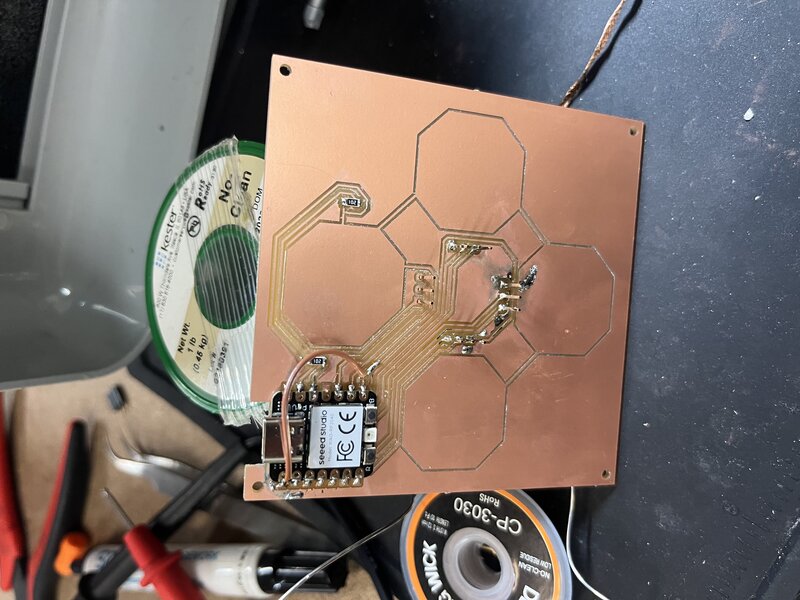
I sanded the edges (my traces were so clean I didn’t really need to sand them!), washed the board, and ended up with this:
Assembling
First of all, I immediately noticed that I had made a mistake in my schematic. I have one pin (called “RX” in my schematic) which needs to do analog reads, but is connected to D7, which is a pin that cannot perform analog reads. I cut the D7 trace (bottom right on the RP2040) and soldered a jumper wire to D0 (top left on the RP2040) instead, which is an unused pin that can perform analog reads.
I was also not sure what resistors to use for my voltage divider. Ben and I talked about it, and concluded that it doesn’t really matter so long as they are equal, so I arbitrarily chose to use 1k resistors. However, later I talked to Quentin and he said that I need to use 1M resistors to slow down the mutual capacitance phenomenon enough to be measurable.
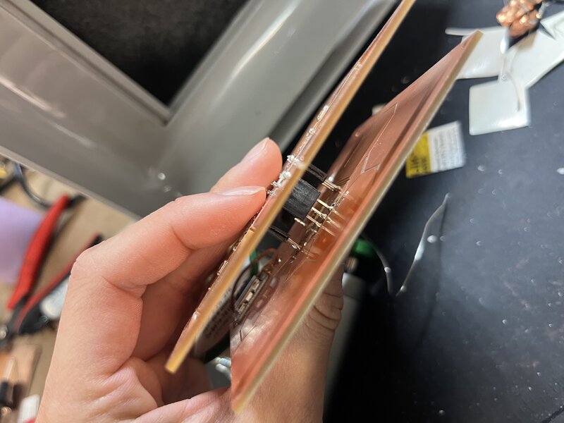
Kristof gave me the brilliant idea to add a male header to one board and a female header to the other so my PCB sandwich can be easily disassembled for debugging. He also showed me how to use the male headers on the bottom board, push the pins all the way in so that they click, then sauter from the top of the board in order to ensure that the pins and their connected nets will make good contact with the female headers on the top panel.
Here is my initial assembly of the base plate, with the wrong resistors (which I swapped out later):
I used the continuity mode on the multimeter to make sure everything was connected as I expected before moving on.
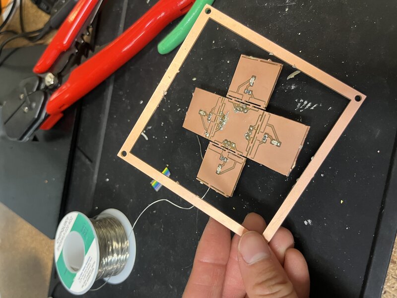
For the arrow plate with the LEDs, I used two red and two blue LEDs to imitate the traditional DDR configuration, where the up and down arrows are red and the left and right arrows are blue. Kristof showed me how to use diode mode on the multimeter (Ohm symbol > change mode to diode) to check which direction the diodes should go. If the probes are connected to the LED the right way (black / ground probe to the cathode), the LED will illuminate. I found on both the kinds of diodes I was using that the small green marks on one end were at the cathode. For the top of the arrow board, I sautered the diodes and double checked that they were connected the right way using the multimeter.
On the bottom face of the arrow board, I stripped wires, stuck the wire through TX hole, put the female header in, and sautered it to the connector pin on the female header from top of the board. I then sautered the other end of the wire to a piece of copper tape. I verified that the female headers make connections to the traces with the continuity mode.
![]()
![]()
With my handy dandy connector headers, I was able to slot the two pieces together fairly easily:

Coding
With the Sandwich assembled, I was ready to implement the code to read the mutual capacitance. To start out, I made the minimal adaptations to Neil’s code for mutual capacitance sensing to read signal from my sensor. Basically all this entailed was changing the pin numbers to match my setup. Turns out, the Seeed Xiao RP2040 uses the MicroPython pin numbers from the pinout diagram – e.g, P0 on the datasheet – instead of A0, D0, etc. After figuring this out and also figuring out how to open the serial plotter, I was able to get signal from my sensor!
Notably, the signal was extremely noisy with nothing but a big air gap between the plates, but it worked a lot better when I stuck my finger in between. Quentin hypothesized that this was because the dielectric constant of air is very low, and capacitance is linearly correlated to the dielectric constant. The dielectric constant of a finger, which is mostly water, is much higher. Quentin found me a nice piece of rubber to put between my two plates. After careful disassembly and reassembly, the signal was a bit better but still pretty noisy, and very affected by e.g. a finger underneath the entire PCB.
Quentin and Kristof suggested I try the following:
- ground the floating parts of the PCB (received a gently stern lecture from Quentin about how ungrounded parts on the PCB are an electrical engineer’s worst nightmare)
- try putting the copper tape + wire directly on the rubber pad and using that as the TX instead
- apply force directly onto rubber with some hard surface
When the CBA gods tell you to do something, you do it. Thus began a fever dream of deeply inelegant electrical engineering.
Something something Ship of Theseus (disassembling + reassembling)
First, I made these sauter bridges to ground the floating parts of my PCB.

I also cut the arrows out of their frame and took the copper tape off the underside off of them so I could use them as the hard surface for depressing the rubber pads.
I sautered jumpers to copper tape on the rubber pads and tested that it worked. In fact the signal was less noisy than before!
I put another rubber pad underneath the base to try to insulate it from confounding fingers which would mess with the signal. I put the original copper frame underneath and screwed the whole thing together so the rubber pad doesn’t move around.
Here’s a cute video of Dan being nosy.
Once I’d remade my entire sandwich, I turned the whole thing on and found that two of the LED pins were disconnected. Unfortunately, the LED connections were broken inside the sandwich, so in order to fix it I would have to completely disassemble and reassemble.

So, I did. Two hours and several incredibly dubious jumper wires later, all the connections were connected! The multimeter and I became intimate friends.

It’s alive! (more coding)
In the name of spiral design, I implemented the code iteratively: 1. First, I wrote blink code to make sure I could talk to all my LEDs. 2. Next, I did some refactoring and cleanup of Neil’s mutual capacitance code (without changing the functionality), and had a nice piece of code to read the key presses from each of the arrow pads. 3. I hardcoded some baseline values for each arrow and a threshold value, and wrote a function to tell if a pad was “pressed” or not based on whether its value surpassed baseline + threshold. 4. I added a 1-second automatic calibration which sets the baseline values of each pad when the device is booted up based on the readings at rest, so I don’t have to go manually tuning a hardcoded threshold every time.
You can see the final Arduino code here.
Here is the final thing! Woohoo :)