Group Measurement Session
.jpg)
Alan and Nik explained and demonstrated several useful pieces of test equipment. Here are the key takeaways from each measurement tool:
Multimeter
- Ideal for initial circuit checks and basic measurements
- Reports average (or RMS) readings rather than instantaneous voltage
- Additional functions can be accessed using the yellow button on our model
Oscilloscope
- Measures voltage over time
- Particularly useful for inspecting:
- Power rails
- Data lines
- Clock lines
- Important note on probe attenuation:
- Probes are labeled as either 1x or 10x, indicating signal scaling
- If readings seem off (e.g., expecting 5V but seeing 0.5V), verify both probe attenuation and scope settings
Logic Analyzer
- Converts analog voltages into digital logic for signal visualization
- Useful for analyzing:
- Transmit signals
- Receive signals
- Clock signals
- To use the lab's analyzer, download the Saleae Logic 2 software
Electronics Design
Component List
| Component | Value/Type | Quantity | Purpose |
|---|---|---|---|
| XIAO | Seeed Studio XIAO | 1 | Main Controller |
| LED | WS2812B | 1 | RGB Indicator |
| Capacitor | 100nF | 1 | LED Decoupling |
| Button | Tactile Switch | 1 | User Input |
| Resistor | 10kΩ | 4 | Button Pull-up |
Electronic Design Automation (EDA)
Drawing inspiration from previous HTMAA projects while incorporating my own artistic vision, I'm developing a circuit design that emphasizes organic, curved forms. This approach aims to bridge the gap between functional electronics and aesthetic design, particularly focusing on how components can flow naturally across the board.
Design Process in KiCad
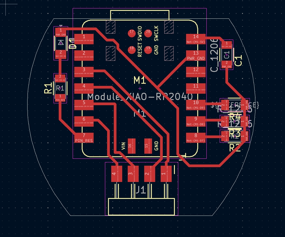
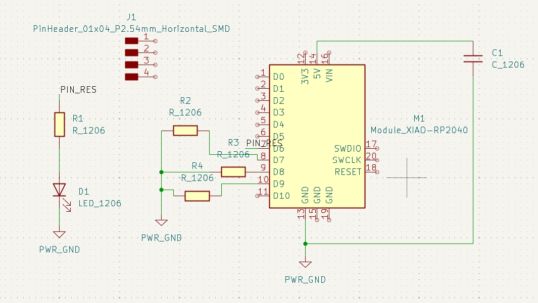
Design Concept
- Input Integration: Incorporating tactile buttons in an intuitive, accessible layout
- Aesthetic Routing: Using curved traces to create a more organic flow between components
- Capacitor Placement: Strategic positioning of capacitors to maintain circuit stability while contributing to the overall design
- LED Arrangement: LEDs placed along curved paths to create visual interest when illuminated
- Future Expansion: Design accommodates future addition of motor components for dynamic movement
Rendered Preview
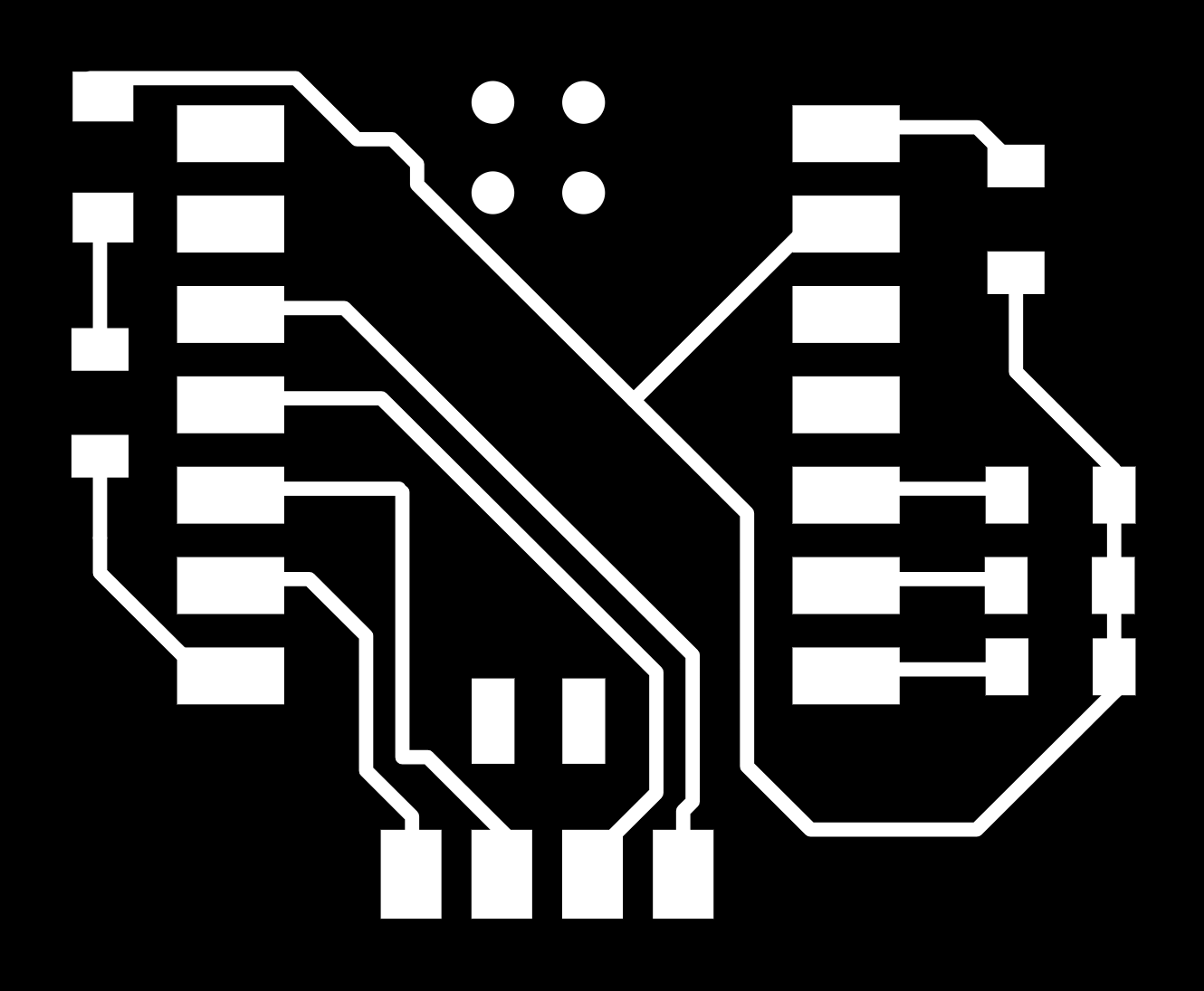
This design represents a departure from traditional PCB layouts, where I'm exploring how electronic components can be arranged in more expressive ways while maintaining their functionality. The future integration of motors will add another dimension to the project, allowing for physical movement to complement the visual design.
Exploring AI-Assisted PCB Design
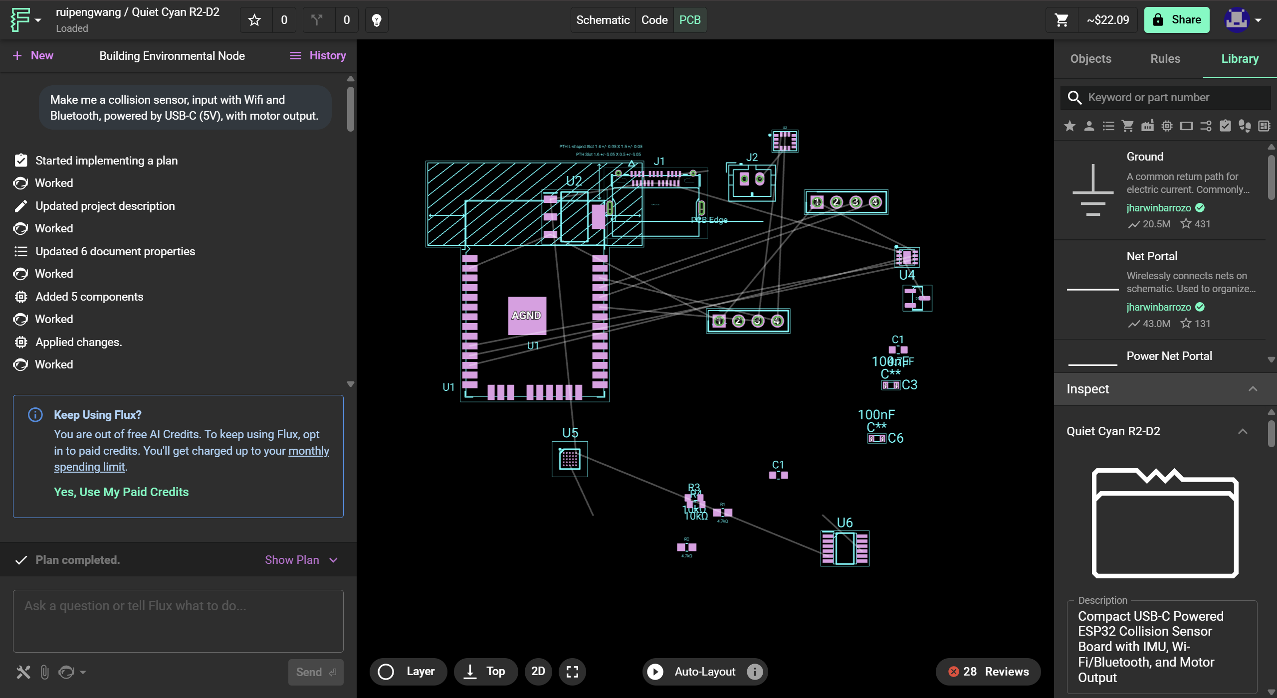
In an attempt to push the boundaries of PCB design further, I experimented with Flux AI, a tool that promises AI-assisted circuit board generation. The goal was to see if AI could help create even more organic and unconventional layouts while maintaining electrical functionality. However, this experiment revealed several interesting challenges:
- Current AI tools struggle with the complex constraints of PCB design:
- Maintaining proper clearances between traces
- Ensuring signal integrity with curved paths
- Balancing aesthetic choices with electrical requirements
- The tool had difficulty interpreting:
- Non-traditional component arrangements
- Artistic routing preferences
- Complex curved geometries
- Learning from the failure:
- Better understanding of PCB design constraints
- Appreciation for the complexity of manual routing
- Insights into current limitations of AI in electronic design
While the AI-assisted approach wasn't successful in this instance, the experiment provided valuable insights into the balance between artistic expression and technical constraints in PCB design. For now, manual routing with careful attention to both aesthetic and functional requirements remains the most effective approach for creating these organic circuit designs.