For the individual assignment, we were tasked with using an EDA tool to design an embedded microcontroller system using parts from the inventory, checking its design rules for fabrication, and simulating its operation. I began by brainstorming projects that were compatible with these constraints. Eventually I landed on a Dimmable Touch Lamp. I have one of these at home, and the fact that it gets triggered by a banana's touch (in addition to human touch) amuses me greatly.
I started out by listing out some TODOs for what would be needed.
Here are the associated inventory items.
| Item | Description | Qty | Unit Price ($) | Subtotal ($) | Link |
|---|---|---|---|---|---|
| SI2336DS-T1-GE3 | MOSFET N-CH 30V 5.2A SOT23-3 | 1 | 0.34 | 0.34 | DigiKey |
| VEL05US050-US-BB | AC/DC WALL MOUNT ADAPTER 5V 5W | 1 | 4.50 | 4.50 | DigiKey |
| PT15-21C/TR8 | SENSOR PHOTO 940NM TOP VIEW 1206 VISIBLE | 1 | 0.10 | 0.10 | DigiKey |
| QBLP650-IW | LED WHITE DIFFUSED 1206 SMD | 1 | 0.20 | 0.20 | DigiKey |
| 102010428 | SEEED STUDIO XIAO RP2040 | 1 | 5.40 | 5.40 | DigiKey |
| Grand Total ($) | 10.54 | ||||
I will also need a resistor. The resistance will be determined later. In a bright room, I would want the ADC reading to be close to its maximum.
I am designing the board in KiCAD. Once I've done so, I will check the board's design rules for fabrication. Quentin's recitation helped teach me some important things. In particular, there is a KiCAD libraries site for HTMAA that needs to be added.
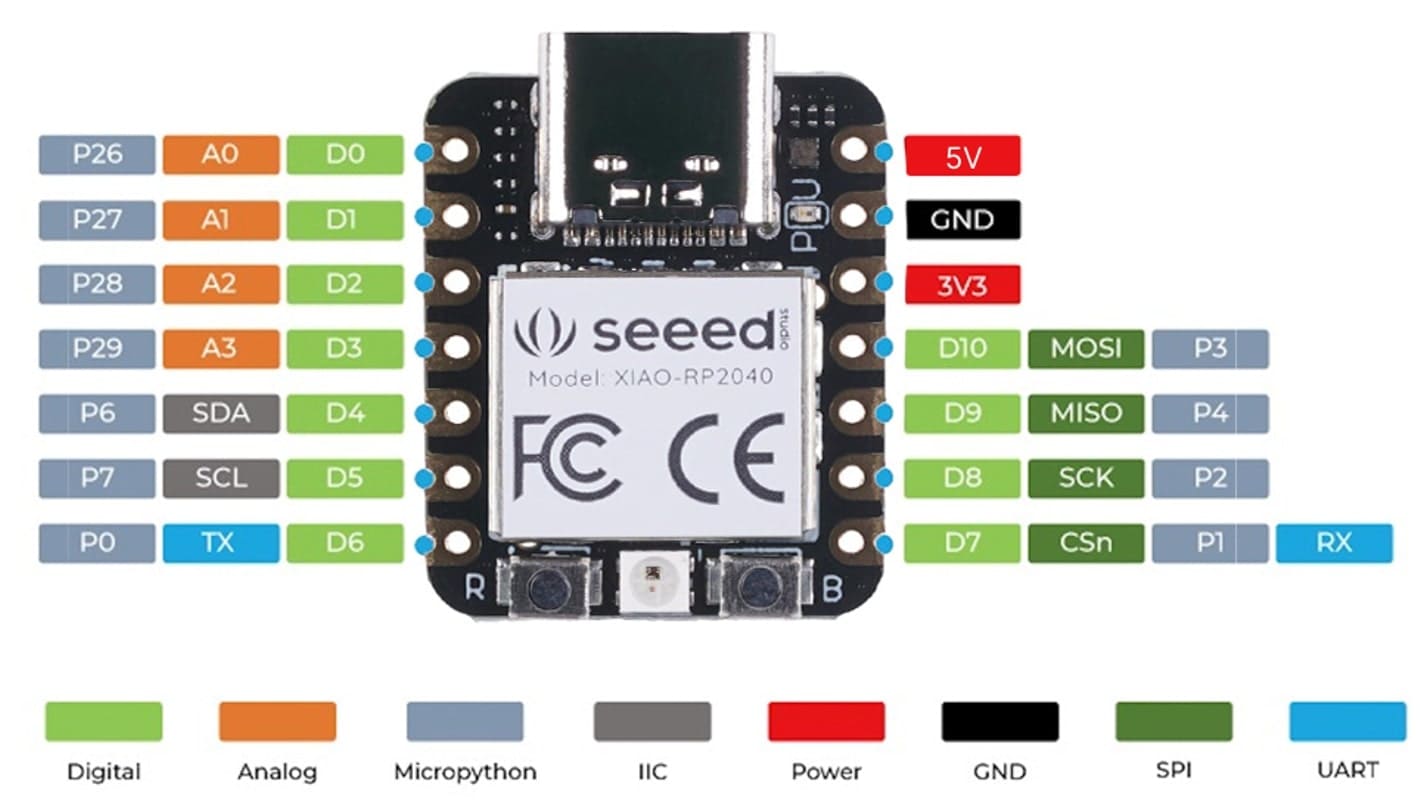
I began by looking at the Seeed Xiao RP2040 datasheet and finding the pinout.
I first added the components from the HTMAA library to the schematic (symbol and footprint) in Preferences.
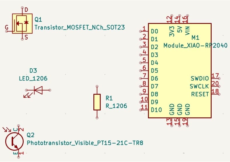
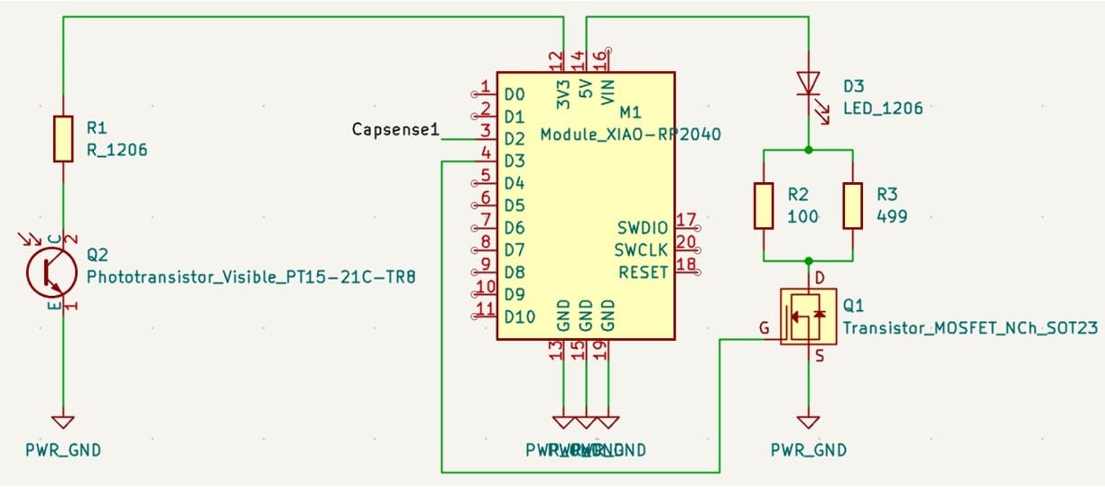
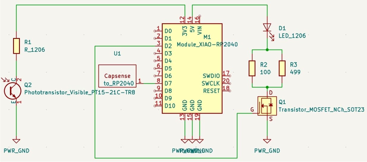
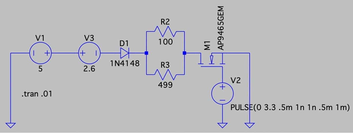
I arranged them properly and added the connections. I also added in two resistors. The voltage drop is 5V - 3.3V = 1.7V. Using this and V = IR where the maximum current is 20mA, I arrived at a desired resistance of 85 Ohms. Since we don't have an 85 Ohm resistor in the inventory, I can create it by putting 100 Ohm and 499 Ohm resistors in parallel.
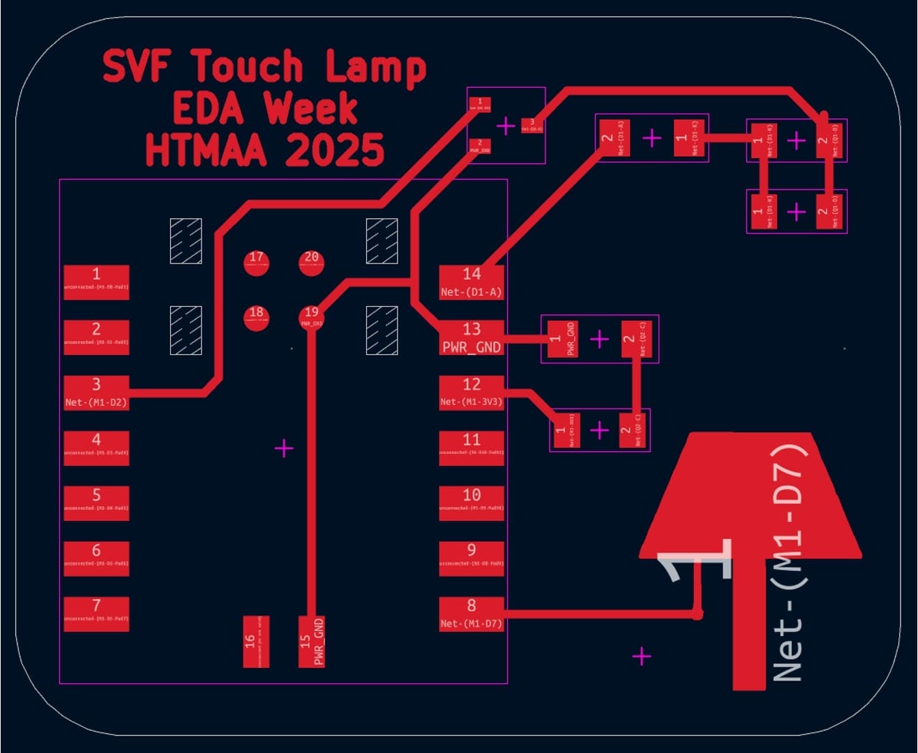
After this, I clicked Tools → Update PCB from Schematic and created the layout. I remembered to edit the minimum clearances and track width to be 0.4mm in the top left corner of the KiCAD screen from Quentin's recitation tips. Once I had done so, I connected everything together with traces. "Control" + "/" allows you to change the curvature of the traces. Here is how that turned out.
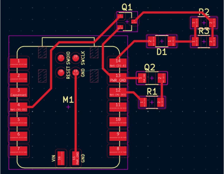
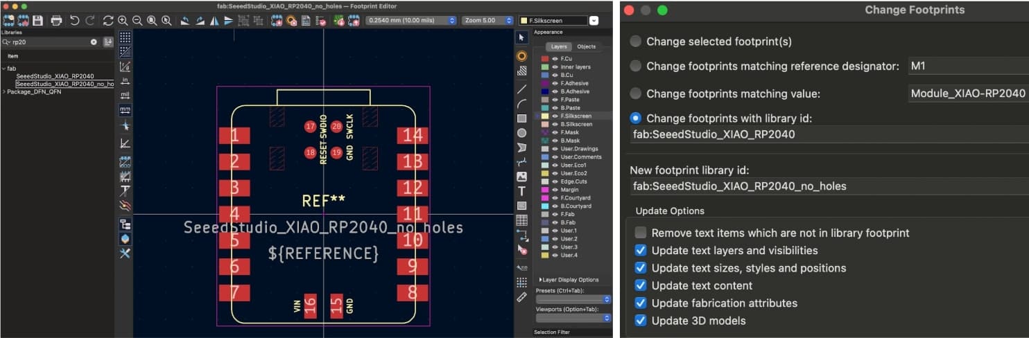
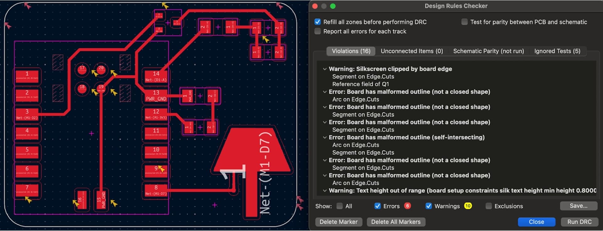
Next came checking design rules. I hit the appropriate button in the top right of the toolbar (it looks like a list with a checkmark on it in my version and like a ladybug with a checkmark in some others) to get started. The warnings about text position don't matter since the silkscreen won’t appear on the milled board anyway. However, I absolutely did need the reminder to add in the touchpad I had created a label for in the schematic. Good catch KiCAD Design Checker! I also edited the footprint of the Seeed Xiao RP2040 to remove the through holes and updated it as shown in the image below.
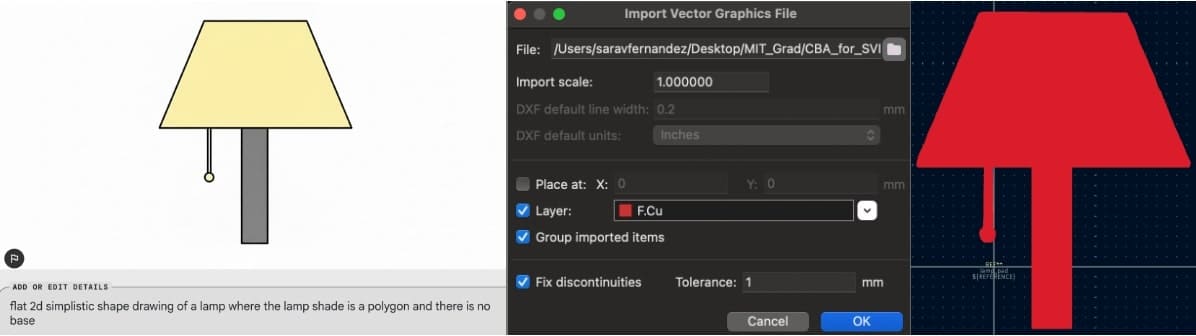
I had the fun idea to make the touchpad look like a lamp. It’s meant to be a touch lamp after all. I went into my favorite AI art generation tool, whisk.fx and input the following prompt: “flat 2d simplistic shape drawing of a lamp where the lamp shade is a polygon and there is no base.” Then I exported the image and removed the background using this handy background remover site. I converted from .png to .svg. To add the image, I hit Footprint Editor → File → Import → Graphics and selected the filepath.
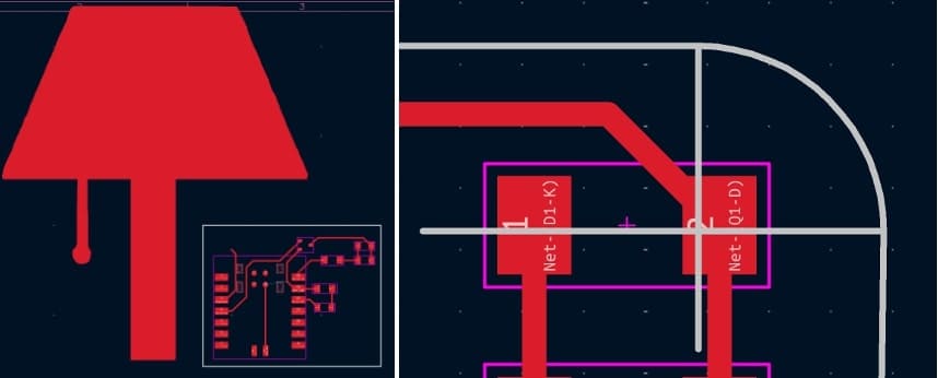
As it turns out, the lamp pad was too large. There didn't seem to be a way to change the scaling of the pad now that it had been created, so I deleted the pad and re-imported with a scaling factor of 0.2 instead of 1. I also added a board outline in the Edge Cuts layer, but the Design Rule Check said that the outline was not properly connected. I put that problem on hold to try solving another one first.
The other problem was that I couldn't figure out how to connect the trace between the lamp pad and any of the pins on the Seeed Xiao RP2040. Naming it the same as the net label of the pin I wanted it to connect to in the schematic did not work, and online tutorials didn't help. In the end, I opted to create my own schematic. I looked to this forum and (more usefully) this YouTube tutorial to get this done. I placed the symbol (Capsense) in the schematic and rerouted pins accordingly.
I had a hard time figuring out how to link this new symbol to the footprint I had created earlier and got some help from Nik. It took some trial and error. Here is the procedure:
Footprint editor → File → New Library (optional) → New Symbol → name the symbol → Add Pad → add other shapes or import image (File → Import → Graphics) → right click → Properties → fill out pad number → make Pad shape Custom → Ok → right click → Edit Pad as Graphic Shape
Symbol editor → File → New Library (optional) → New Symbol → name the symbol → draw the symbol using the toolbar on the right → Draw Pins button → fill out pin properties → Save → Place Symbols → Okay → connect them where desired → E on keyboard → add footprint to Footprints.
Next, I tried fixing the board outline discontinuities following this curved board outline tutorial. Although I painstakingly drew every line as precisely as I could, since grid snapping was disabled, I got the same errors as before in the Design Rules Check.
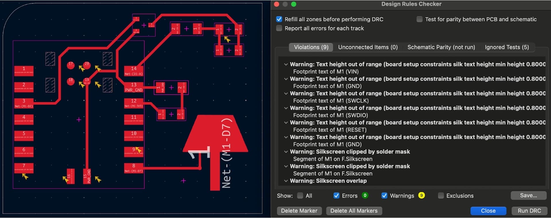
Although I couldn't find a place to explicitly turn on grid snapping, Dimitar suggested I increase the grid size, using the button in the top right of the PCB editor. In the spirit of working in small spirals, I made a single curved corner and ran the Design Rules Checker again, and all looked good! (The only warnings were about the silkscreen, which again doesn't matter in this case.)
I then did the same for the remaining corners. This is how I did this. On the Edge Cuts layer at 100mils grid size, draw a 45 degree angle line cutting off the corner. Draw lines from the points at which the intersection occurs on the outline towards each other such that a new intersection is formed, creating a little square. Ensure snap-to-grid is maintained. Use the arc tool starting at that most recent intersection you created, click on the intersections with the board outline you created in turn, delete the construction lines, and then redraw in the remainder of the outline.
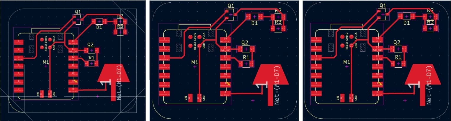
I had initially wanted to put the LED directly above the lamp pad, but I was warned to move the light away because the electric field coming from the trace that carries power for the LED will get picked up by the capacitive sensor. I added some final touches such as text on the F.Cu layer with 0.3mm thickness, which should be millable by the Carvera. The Design Rule Check told me the outline was still not connected properly (likely due to slight misclicks when placing the arcs). I quickly fixed that and did a final Design Rule Check. All is good now!
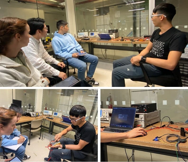
Alan and Nik explained and demonstrated several useful pieces of test equipment. Some takeaways from this are as follows. A multimeter is good for initial checks but will measure average, not absolute, voltage. Additional functionality can be accessed using the yellow button on our particular model. Oscilloscopes measure voltage over time and are useful for looking at power rails, data lines, and clock lines. Crucially, probes are labeled as 1x or 10x, which indicates the amount of voltage attenuation. If you expect to see 5V and see 0.5V, this may be why. We also looked at a logic analyzer which decodes voltages into digital logic. This is useful for seeing digital peripherals like transmit, receive, and clock. To use the one in the lab, we will need to download the Salaea Logic 2 software. Others' takes on this session can be found on this week's CBA group site.
Next came simulation. I looked at the ngspice site which is compatible with KiCAD (and open source) provided a YouTube intro and tutorial. However, I opted to use LTspice which felt much more intuitive albeit simplistic. I added the relevant parts of my schematic and right clicked on the symbols to change their values and names. In advanced settings for V2, I made a PWM voltage source and created a stand-in for my LED using the 1N4148 diode in the LTspice library plus an additional voltage drop of 2.6V. On a Mac, you need to manually tell LTspice that there will be a simulation. To do so, right click → Draft → SPICE directive → type in “.tran .01” and it should work.
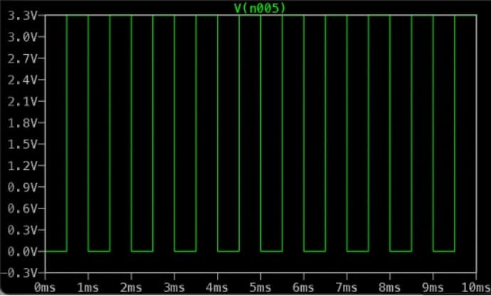
After this, I right clicked and hit Run to run the simulation and begin probing. Probing above V2, I expect to see a square wave from 0 to 3.3V.
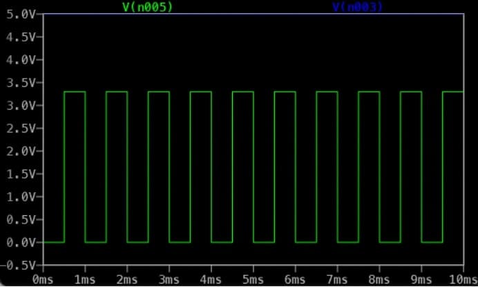
Probing to the left of V3 I also expect to see a square wave from 0 to 3.3V. The scaling is different here, but the result is as expected.
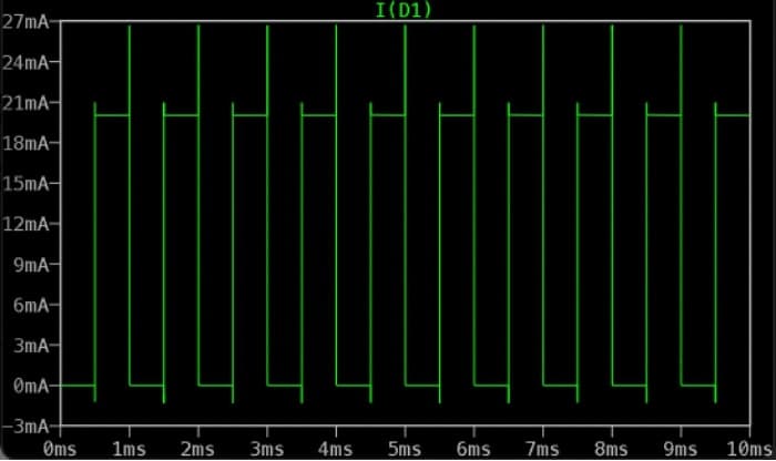
Probing the diode D1, I expect to see a square wave with spikes due to internal capacitance of the MOSFET. This may not exactly match the real-world performance due to the simulation’s inherent limitations.
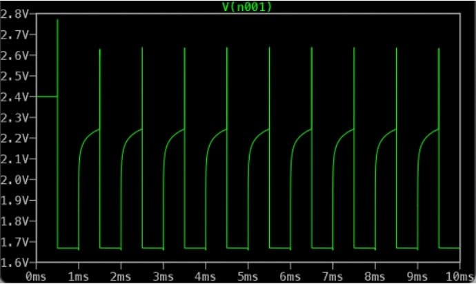
Probing before the resistors, I expect there to be a voltage square wave, defined by 1.7V. When the MOSFET is off, however, the voltage floats on the MOSFET’s capacitance.
I am glad to have gotten more practice using these simulations and am curious to see how much they deviate from reality once I mill out my board next week. I look forward to learning more soon.
Design files can be downloaded here: Download Week05_HTMAA.kicad_sch. Download Week05_HTMAA.kicad_pcb. Download partial_lamp_sim.asc.