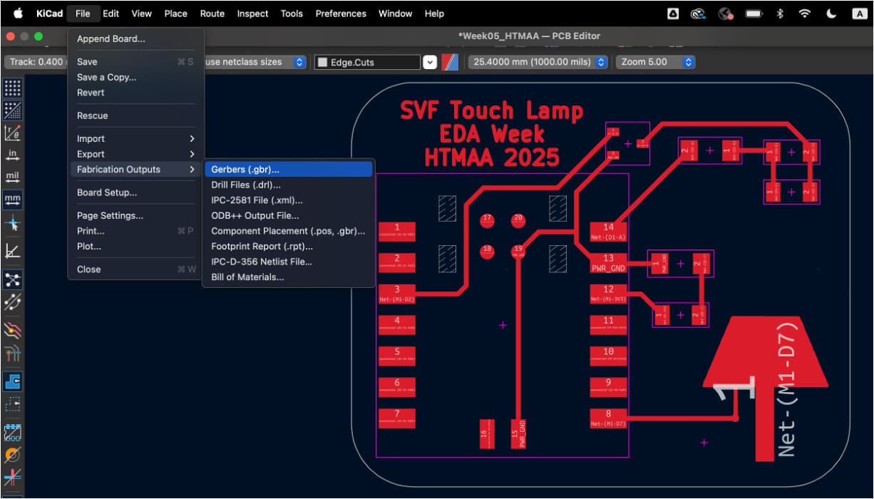
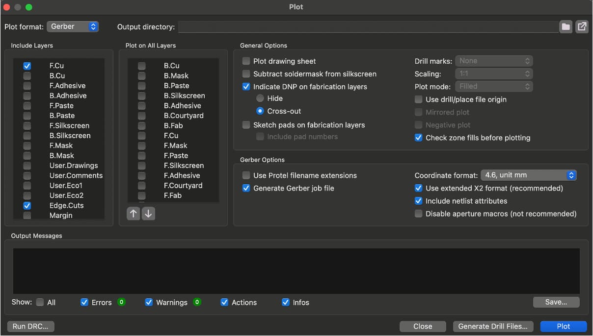
I followed Quentin's Carvera PCB Tutorial for much of this week. I exported the gerber files for the F.Cu and Edge Cuts layers.
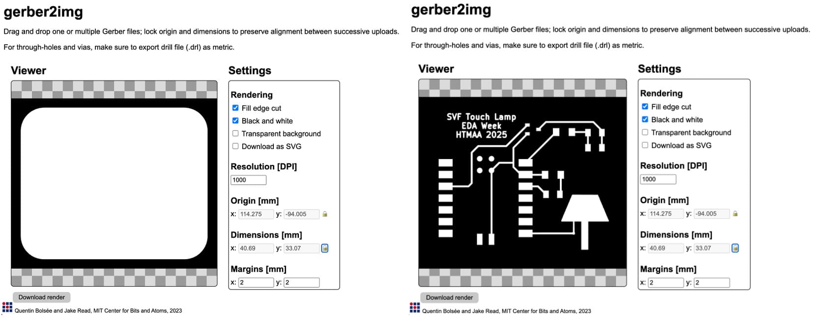
I then went to Quentin's gerber2img site and dragged in the edge cuts gerber file, making sure to lock the origin and dimensions by clicking on the two locks after dragging in the file. Then I downloaded the image, dragged in the traces gerber file, and downloaded the second image.
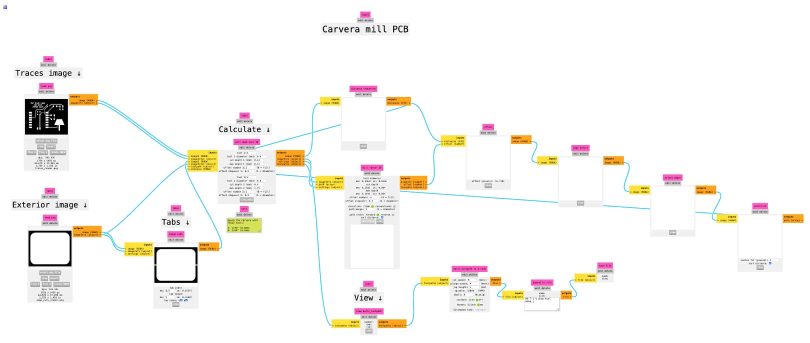
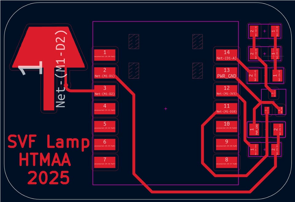
I opened up mods and uploaded the images. I hit calculate as described in Quentin's tutorial and it generated toolpaths for me.
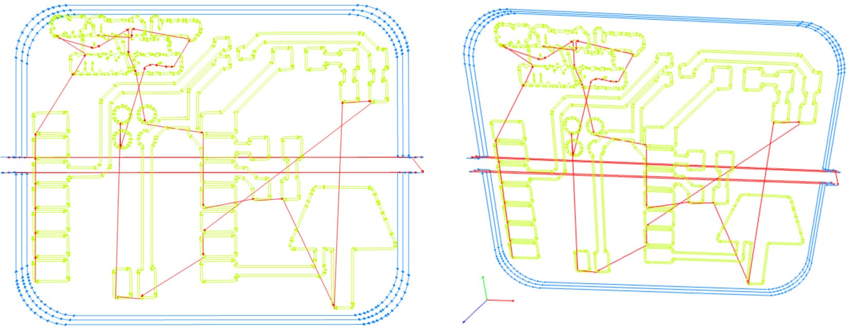
I rotated the toolpath depiction to make sure that the edge cuts were leaving enough margin for the traces, and they were. The lettering was clearly not going to come out right, so I spent some time adjusting font types and sizes. I landed on Avenir Next Ultralight with a size of 1.6 at this stage (but spoiler, it still didn't work very well).
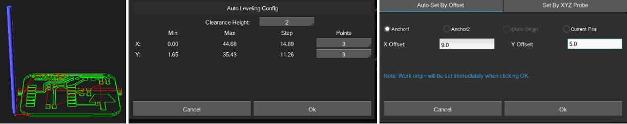
I then took my flashdrive over to the Carvera and set up the job. After clicking the bottom-leftmost button, I uploaded my .nc file and selected it. This made the toolpaths get displayed on the screen. Then I hit the gear icon on the lower left, followed by configuring autoleeling and offset. This is described in further detail in Quentin's tutorial.
I secured the copper clad (single-sided FR1 board) and ran the program. I confirmed the probe outline was correct which meant my measurements were accurate.
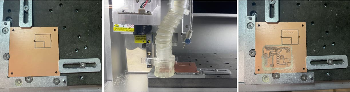
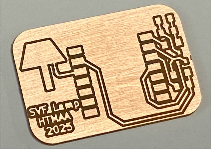
The surface finish was worse than I expected, so I asked for guidance as to whether or not to replace the endmill. I was advised to wash and sandpaper it and see what happens. I think it turned out quite well after that. The letters were still not legible though unfortunately.
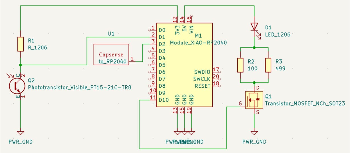
I collected the components I would need to solder and took another look at my design. As it turns out, the phototransistor wasn't connected to a pin that could read information from it, so I needed to modify the board design. At least it gave me an excuse to fix the lettering problem.
The changes that needed to be made were as follows, with motivation and further explanation in parentheses:
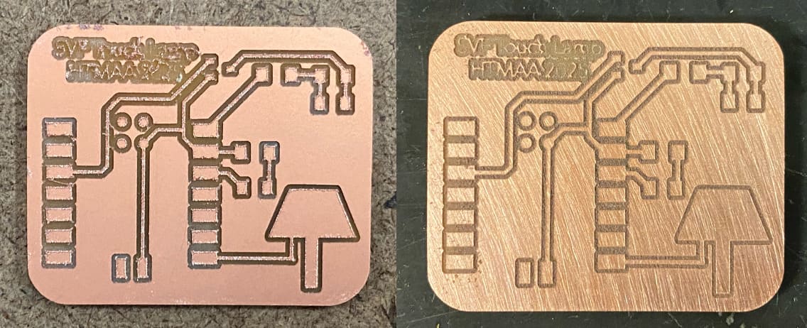
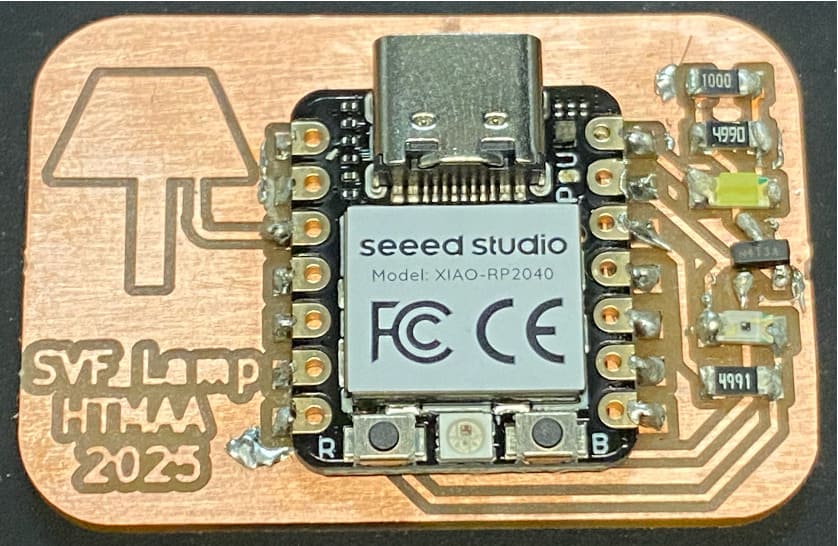
I went through and followed the Carvera PCB milling process again and quickly got the milled board. After washing and sandpapering, it looked like this. The lettering came out well.
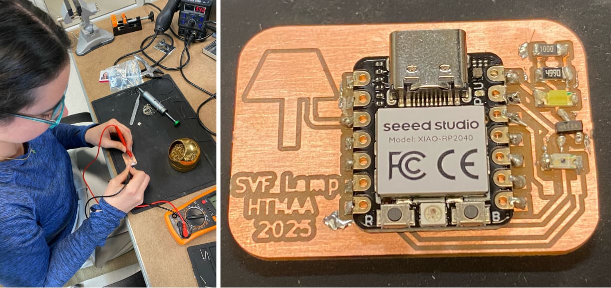
I got my small bag of components and got to soldering. I refered to my schematic to remind myself what went where and checked datasheets to check orientations. To be extra sure, I used a multimeter to confirm the direction of the LED before I placed it and then again once it had been soldered on.
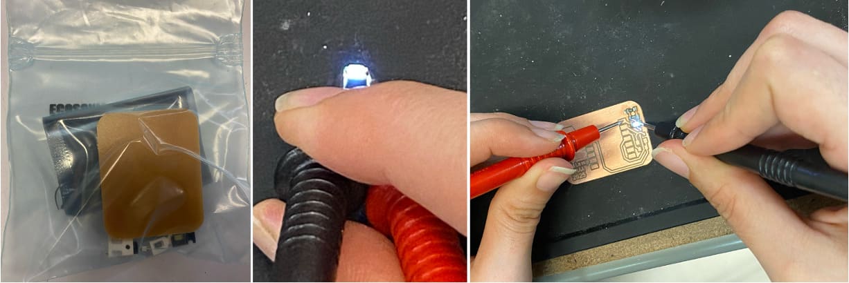
Thank you to Jacqueline who helped me get some action shots of this. I went on to solder the remainder of the components, confirming the direction of the phototransistor as well. The last component that would need to be selected and soldered onto the board was the final resistor.
I plugged in the Seeed Xiao RP2040 and used a multimeter to measure current passing through where the resistor would be when shining a light from iPhone onto the phototransistor. (All the connections looked good when I tested with a multimeter, so I thought it would be find to plug in the Seeed Xiao RP2040 to power it on.) Protip, make sure you flash the RP2040 before you add it to your circuit since it is pre-flashed with an odd pinout. Because of this it caused there to be a strange readout initially. Once I fixed that by resetting the pin to default settings in the Arduino IDE (by adding the line int value = analogRead(A0);), the current value I was trying to measure came out to be ~0.5mA. Therefore, the current isn't likely to exceed ~1mA. Since V = IR, 3.3V - (~1mA)*R should be greater than zero. You also want to maximize R to get higher sensitivity. Therefore R can be ~3k Ohms. Since we don't have a 3k Ohm resistor in the inventory, a 4.99k Ohm resistor will do just fine. With this determination in mind, I secured the final resistor and added it to the board.
Now that I had a completed board, I set out to write code for it. I wrote pseudocode in the Arduino IDE and then started by assigning pins since the startup defaults were different than I expected. My pseudocode included placeholders for both the capacitive sensing and light measurement functionalities.
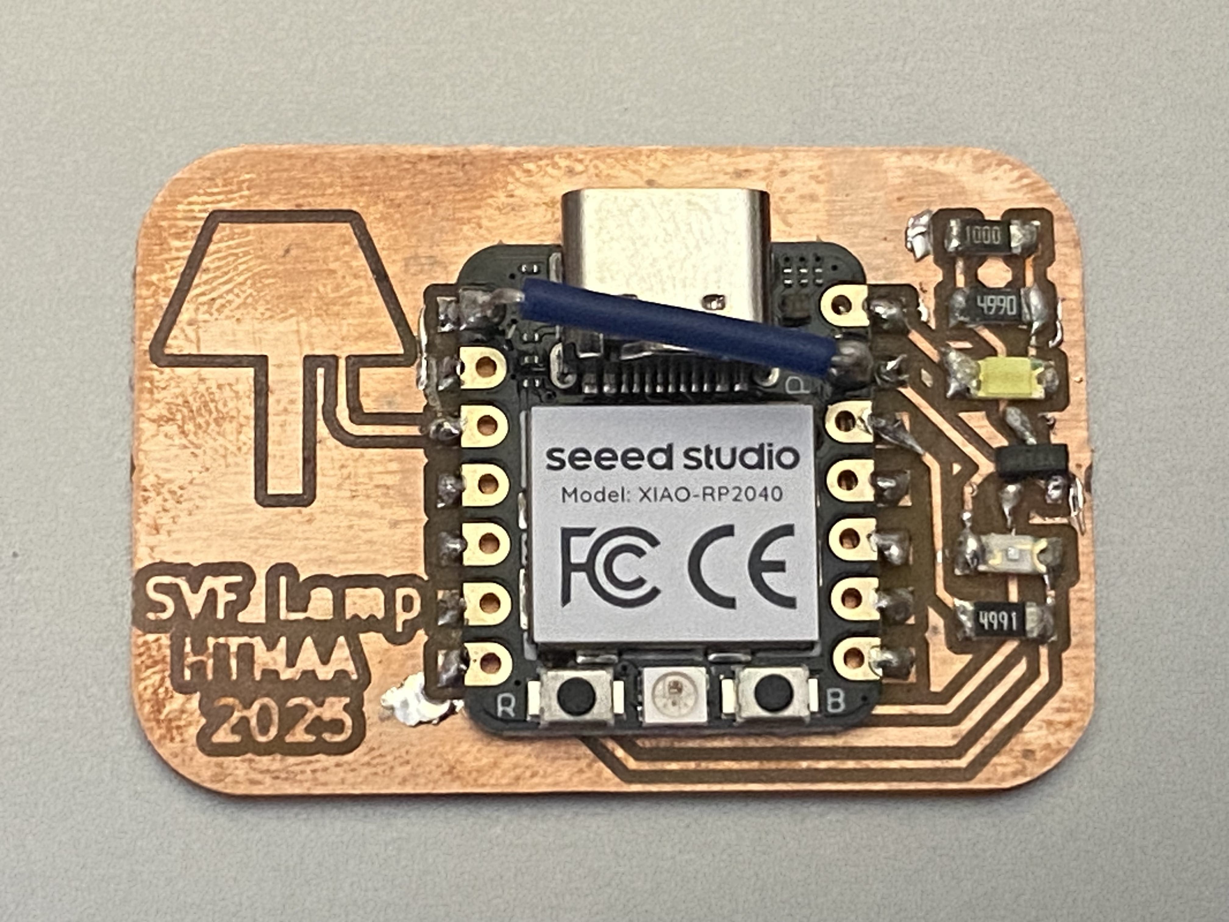
In the process of assigning pins, I realized I would need an additional GND pin and soldered on a wire accordingly.
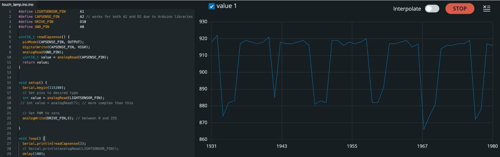
Once I had some code written for the light sensor, I plugged in the Seeed Xiao RP2040 and tried to upload the code to it. I had a lot of trouble getting my computer to recognize the port. This was fixed by using a USB-C to USB-C cable rather than using a USB-A adapter for my USB-C-using Mac connected to a USB-A to USB-C cable. This had worked in the past but didn't this time for some reason. I opened up the Serial Plotter in Tools to see the behavior in real time. I covered the phototransistor (dark condition) and uncovered it (light condition) as well as turned the room lights on and off, which generated this behavior. When the room gets darker the voltage goes up. The opposite happens when you shine a bright light on it. When the room is darker, the light on the board gets brighter. When the room is brighter, the light on the board dims.
I tested some code for the capacitive sensor also, but because of the way the Arduino libraries work, I will need to do something much more complicated to get it to work. I also should have removed the copper near the capacitive sensor. I can work on fixing the code for the capacitive sensing later on given that this week was focused on electronics production more than computation. More making and testing to come!