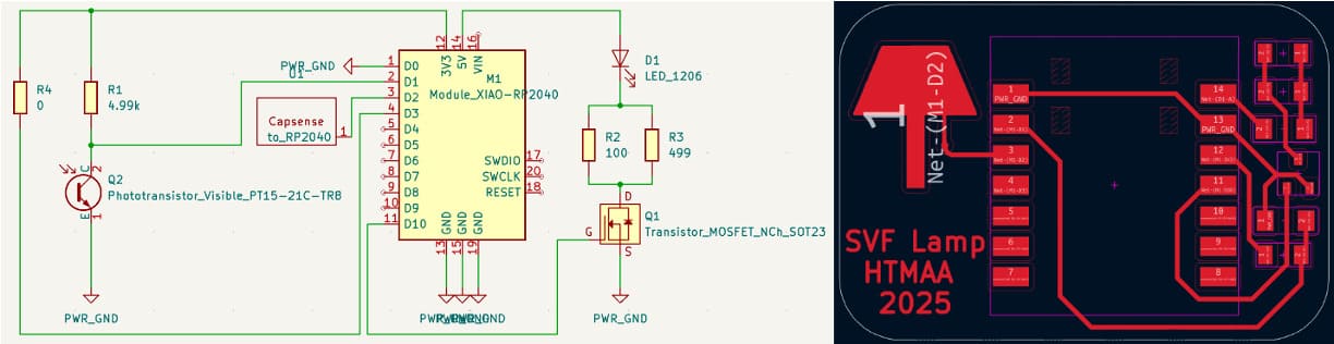
Since I already got the phototransistor measurement working on my touch lamp a couple weeks back, I decided to revisit the capacitance measurement portion of the design to try and get that working. I first updated my schematic and layout to include the connection between A0 and GND I had left out previously. I also would need to connect VDD and A3 and decided to use a jumper wire to do that to not waste too much time rerouting. In the schematic I put in a zero-Ohm resistor, but the layout didn’t really allow for this trick.
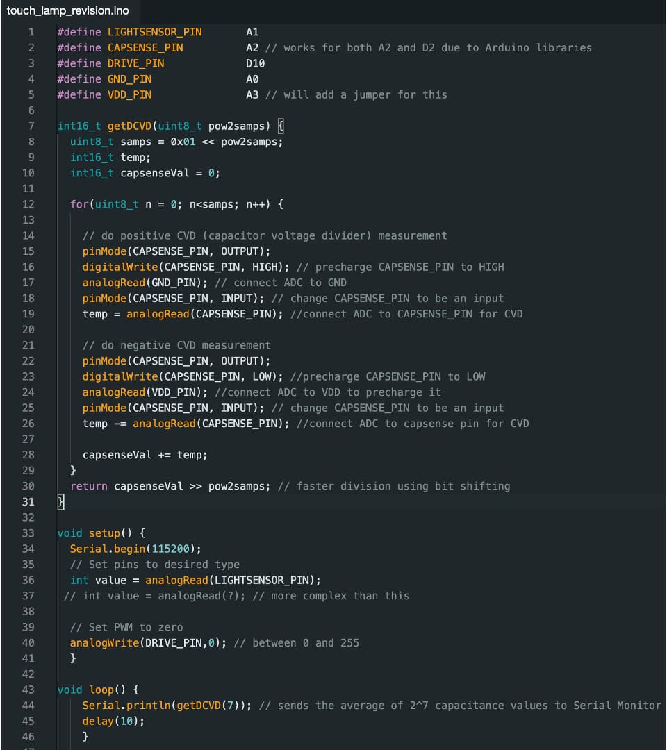
I revised the code for capacitance sensing in isolation rather than trying to get both the phototransistor and capacitance sensing working in tandem for now. Since I had trouble with the capacitor voltage divider (CVD) approach previously, I tried implementing the DCVD (differential CVD) approach to make it work better with less noise.
To do this, I set the external capacitive pad positive, then negative on the second measurement, and then subtracted one from the other. This subtracts out the bias due to systematic error, such as leakage current in the ADC or external fields, and should yield cleaner results. The updated code is here.
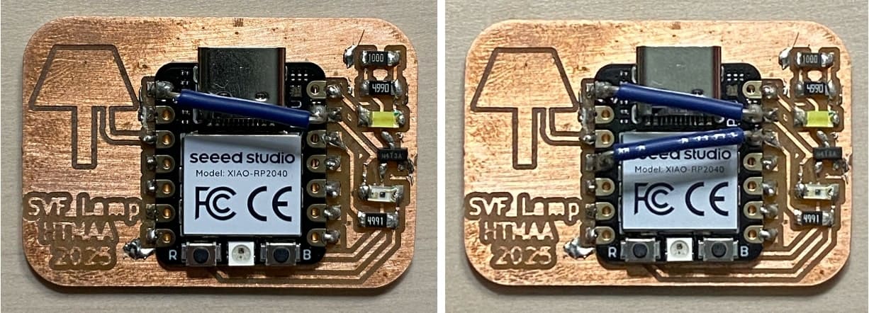
To make sure it’s working properly, I plan to add a jumper connecting VDD and A3 to the board I already have and test it. Here's the board before and after.
I made a few revisions to the code to improve performance. I increased the number inside of getDCVD() to be 12 to increase precision with a higher number of averages and also to avoid increasing the delay. I also included
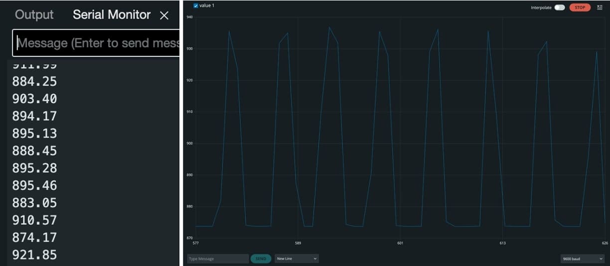
Here's the test. I covered the capacitive sensing pad with tape to prevent shorting with the excess copper I didn't remove when I initially made the board. After checking that the Serial Monitor was outputing reasonable values, I (as periodically as possible), moved my finger away from and then towards the capacitive sensor. The result was reasonable based on my movements, and having changed the code made it so that the noise that was previously obfuscated by lack of precision was actually made visible.
If I were to mill out a new board I would remove all excess copper to reduce unwanted coupling to the capacitive sensor as suggested by Neil during class. If I were to have extra time, I would like to translate that signal into the output of selective LED brightness using pulse-width modulation (PWM), but I'm not sure that I'll get there. Since this week is extremely busy for me, I am strongly leaning into the supply-side time model of working, and so far it's been going well. It just means my project this week will be a little less ambitious.
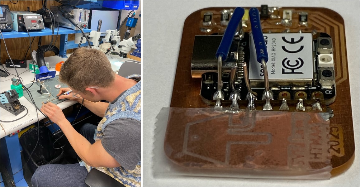
For the group assignment, we were tasked with probing an input device's analog levels and digital signals. Ben offered to teach some of us, so Edward and I joined him to probe my board. First Ben and I soldered on one pin each to make the probing easier, and then we measured the analog signals from my capacitive sensor and phototransistor using a signal analyzer capable of both analog and digital measurements. Analog signals are continuous, whereas digital signals are 1s and 0s. We measured the digital signal from a soil humidity sensor Ben had as well. The group assignment is documented in more detail on our group page.