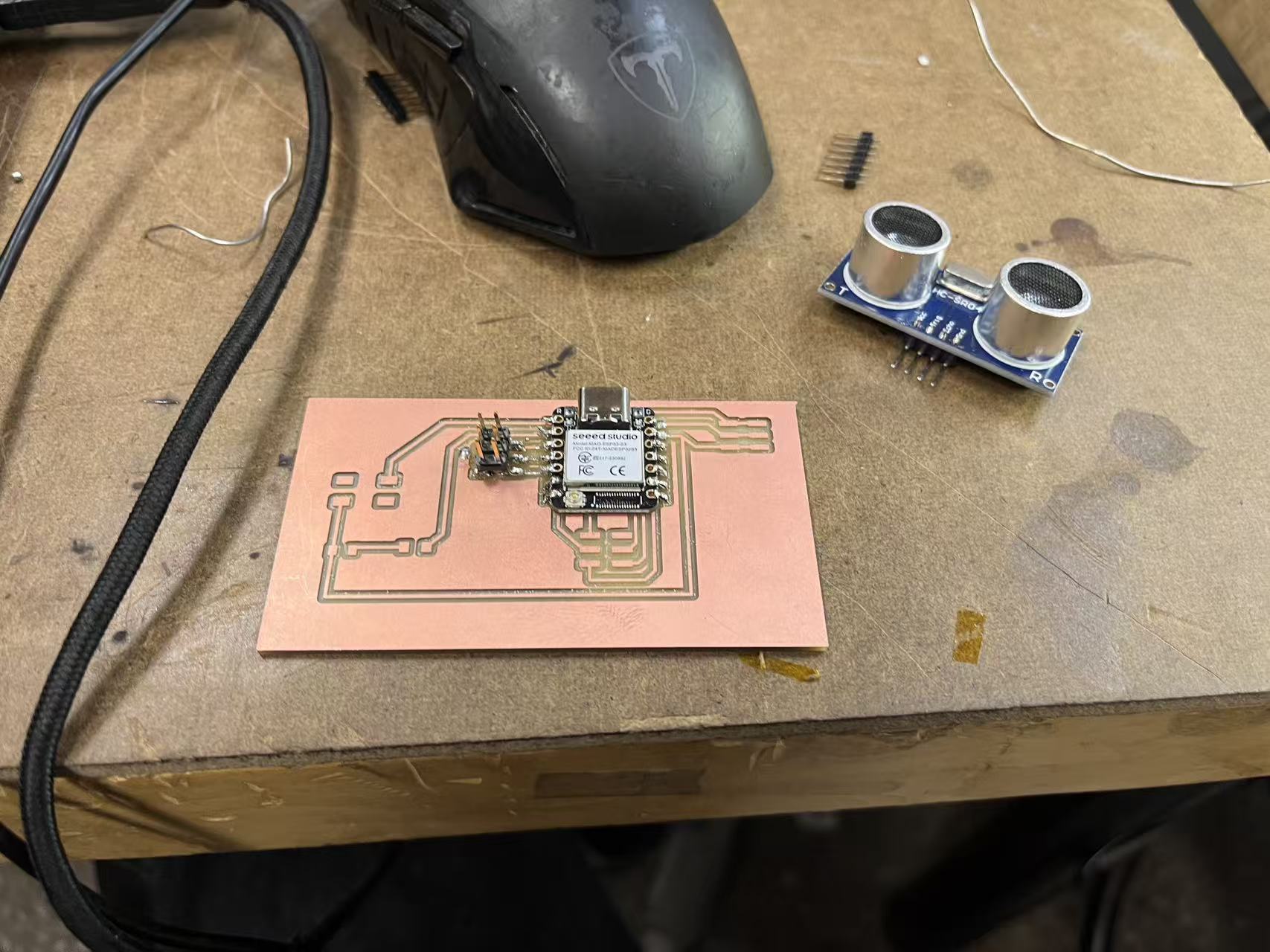
This week was about turning PCB designs into real boards. As a group we characterized our in-house PCB design rules and sent a reference design to a board house. Individually, I went through several failed milling attempts before finally producing and testing my own microcontroller board.

Assignments

  • Group: characterize in-house PCB design rules; submit a PCB to a board house.
  • Individual: make and test an embedded microcontroller board that I designed.

Group assignment (1–3)

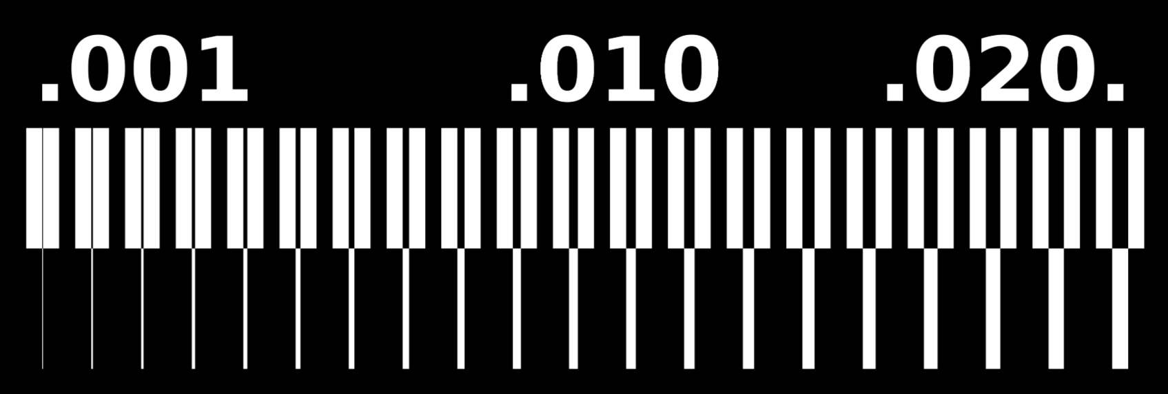
We ran a design-rules check for our in-house mill: measured trace/space and clearance using a calibration ruler, then confirmed what reliably cuts on our copper stock with 1/64″ and 1/32″ tools. In parallel, we exported a reference PCB (Gerbers/NC drill) and submitted it to a board house to compare finish, mask, and solderability.
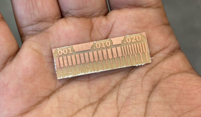
Design rule test cuts and notes
1. Design rule test cuts and notes for minimum trace width and clearance.
DRC ruler layout and milling plan
2. DRC ruler layout showing different trace/space combinations for the mill.
3. Milling the DRC ruler and checking which features survive in copper.

Individual assignment (4–20)

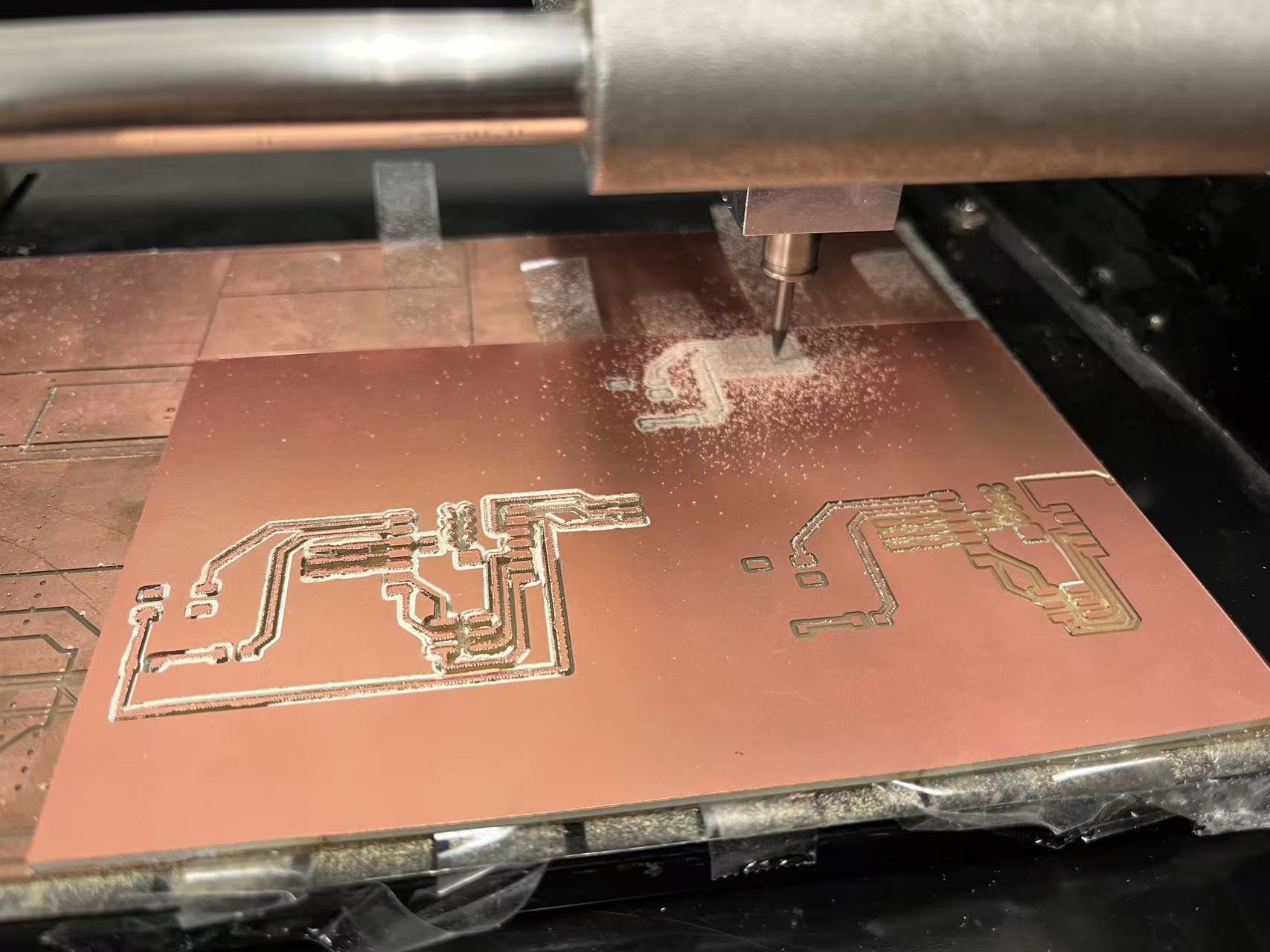
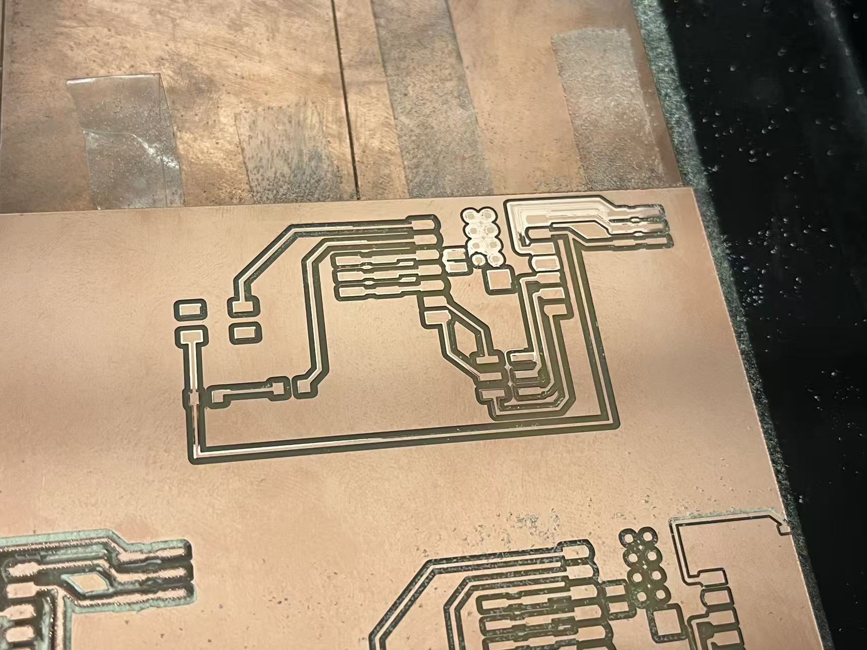
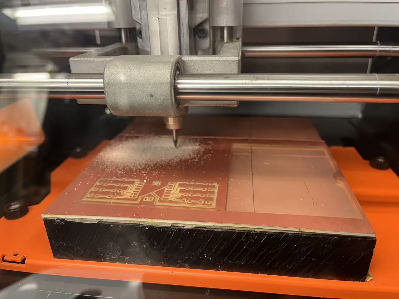
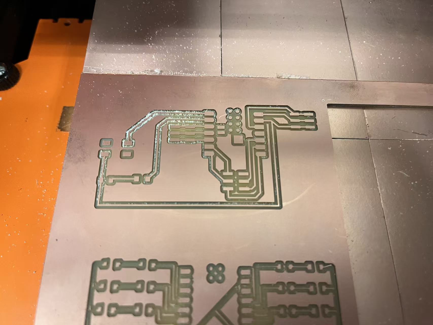
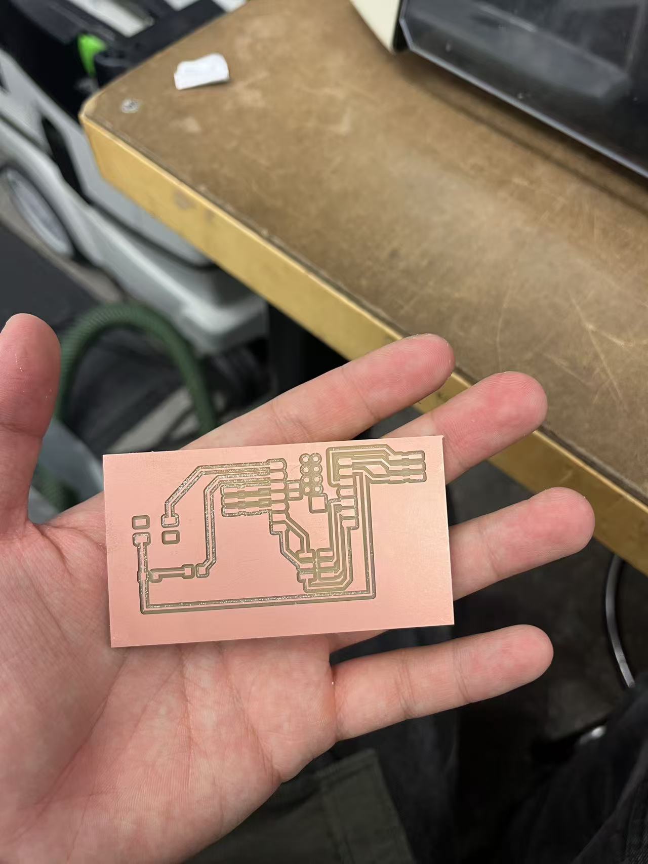
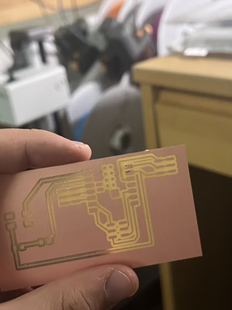
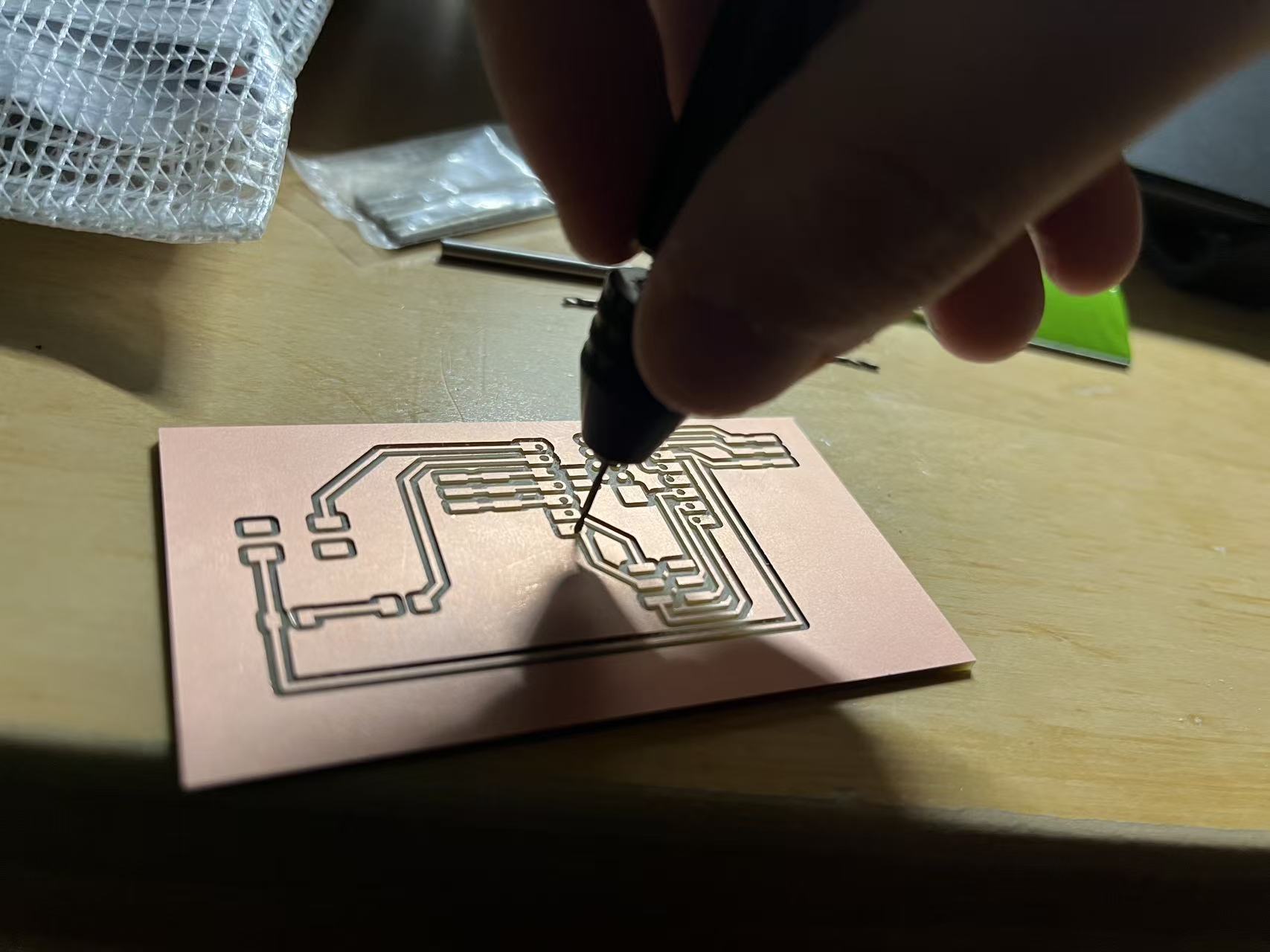
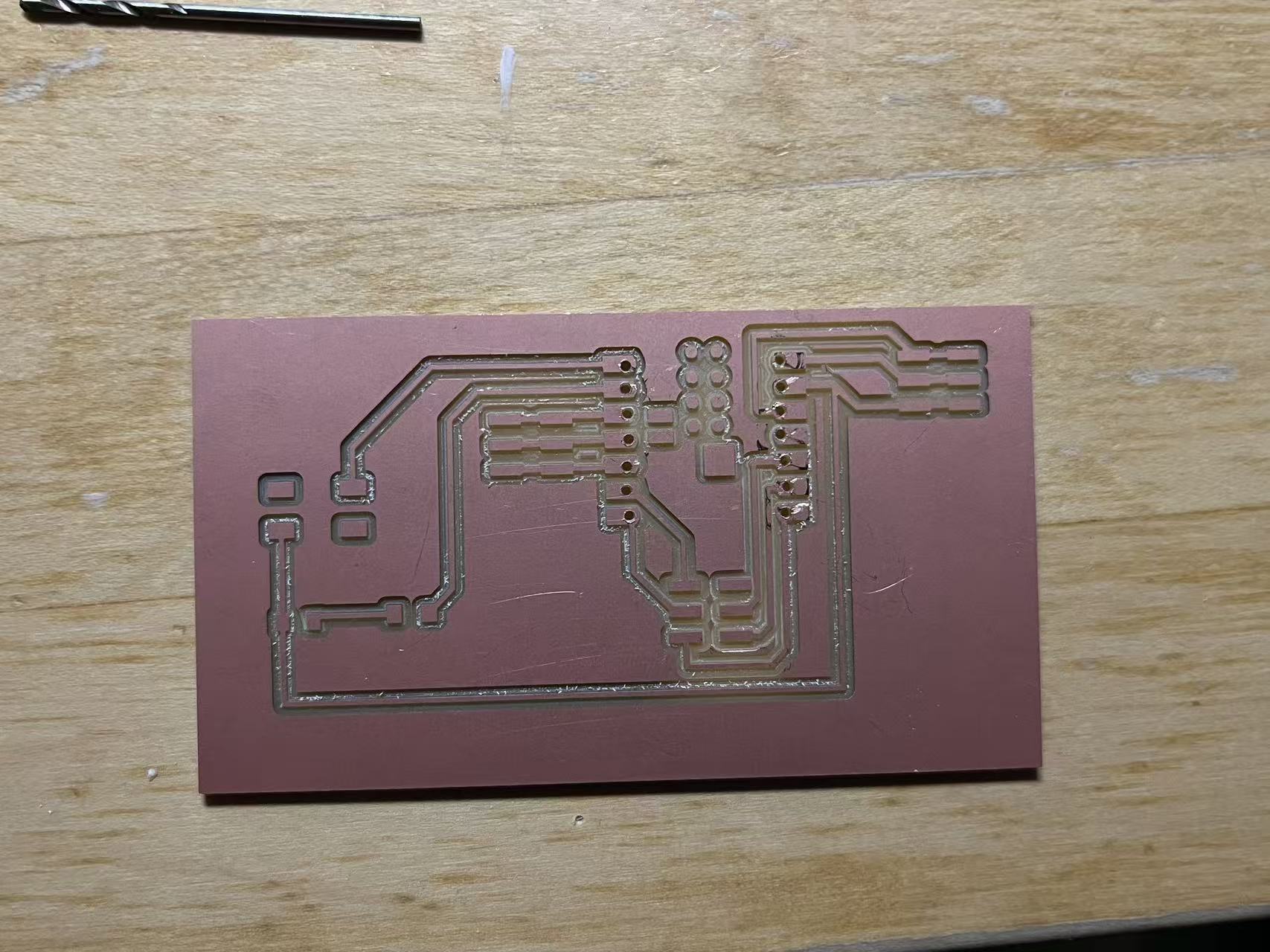
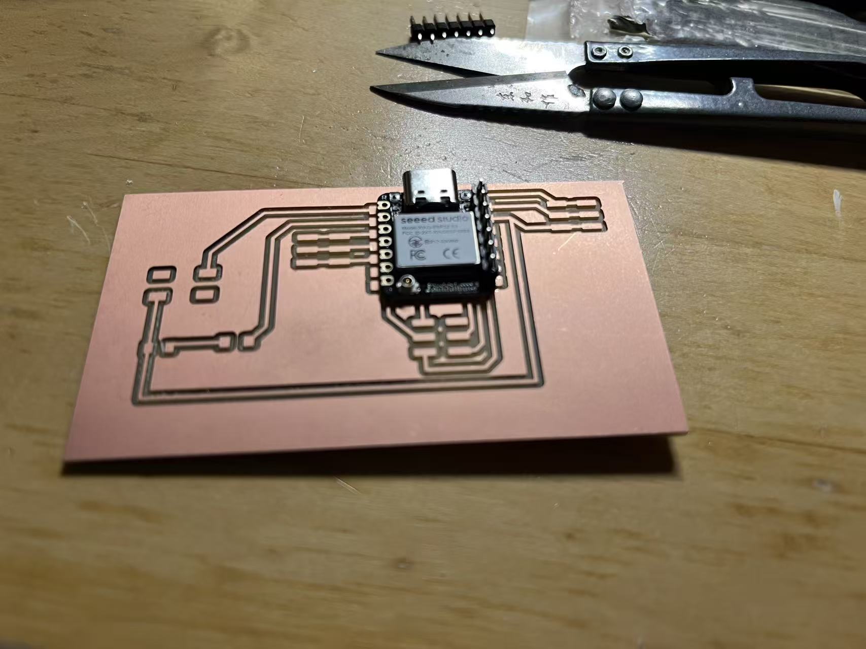
For my own board, I tried to mill a small microcontroller design. I failed multiple times: poor Z-zeroing, worn bits, traces peeling during cleaning, and a couple of shorts from copper dust. After re-leveling the sacrificial layer, replacing the 1/64″ tool, slowing the feed, and increasing clearance in CAM, the board finally milled cleanly. I deburred, checked continuity, then soldered the components and verified power, reset, and USB/UART communication.
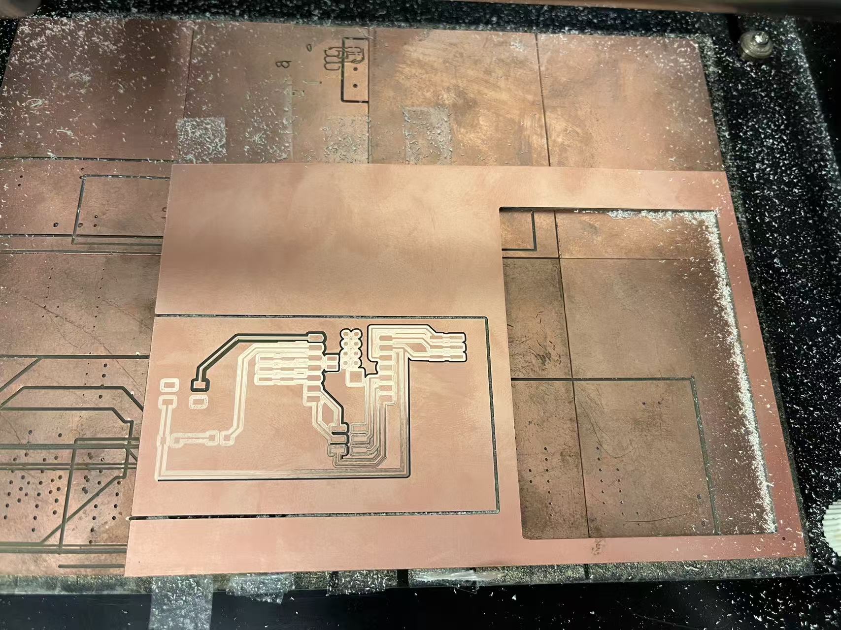
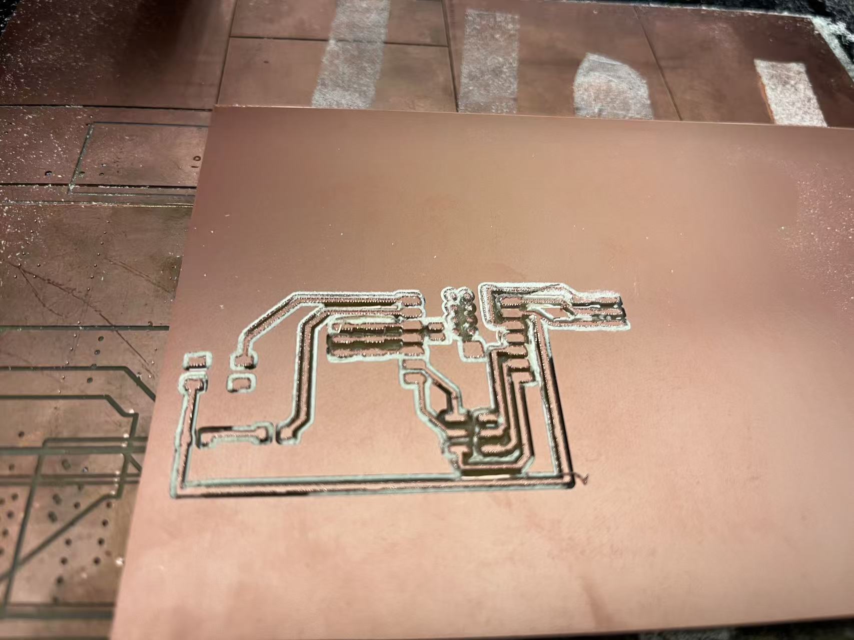
4. First milling attempt—struggling with uneven Z-height across the copper board.
5. Later pass after re-zeroing; traces start to look much cleaner.
Partially milled board with rough traces
6. Early board where some traces milled too shallow and others too deep.
Newly milled board after tool change
7. Fresh cut after changing to a new 1/64″ bit and adjusting feed.
Close-up of broken traces
8. Close-up of broken and lifted traces from one of the failed passes.
Copper board with isolated islands
9. Copper islands where the outline cut too close to signal traces.
Board with visible shorts
10. Visible shorts caused by leftover copper burrs between thin traces.
Re-leveled sacrificial layer
11. Re-leveled sacrificial layer to get a more consistent Z across the board.
Cleanly milled board
12. Finally: a cleanly milled board with all traces intact.
Board after deburring and cleaning
13. Board after deburring, vacuuming, and an IPA wipe to remove dust.
Checking continuity with a multimeter
14. Continuity test between pads to make sure there are no hidden shorts.
Soldering small SMD components
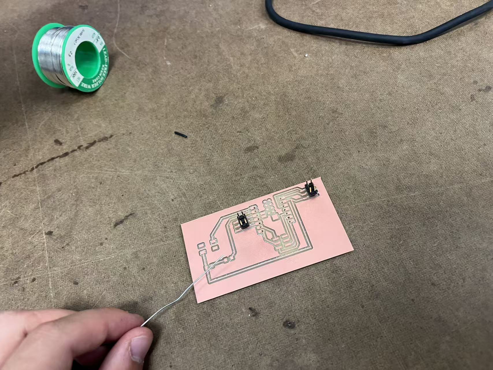
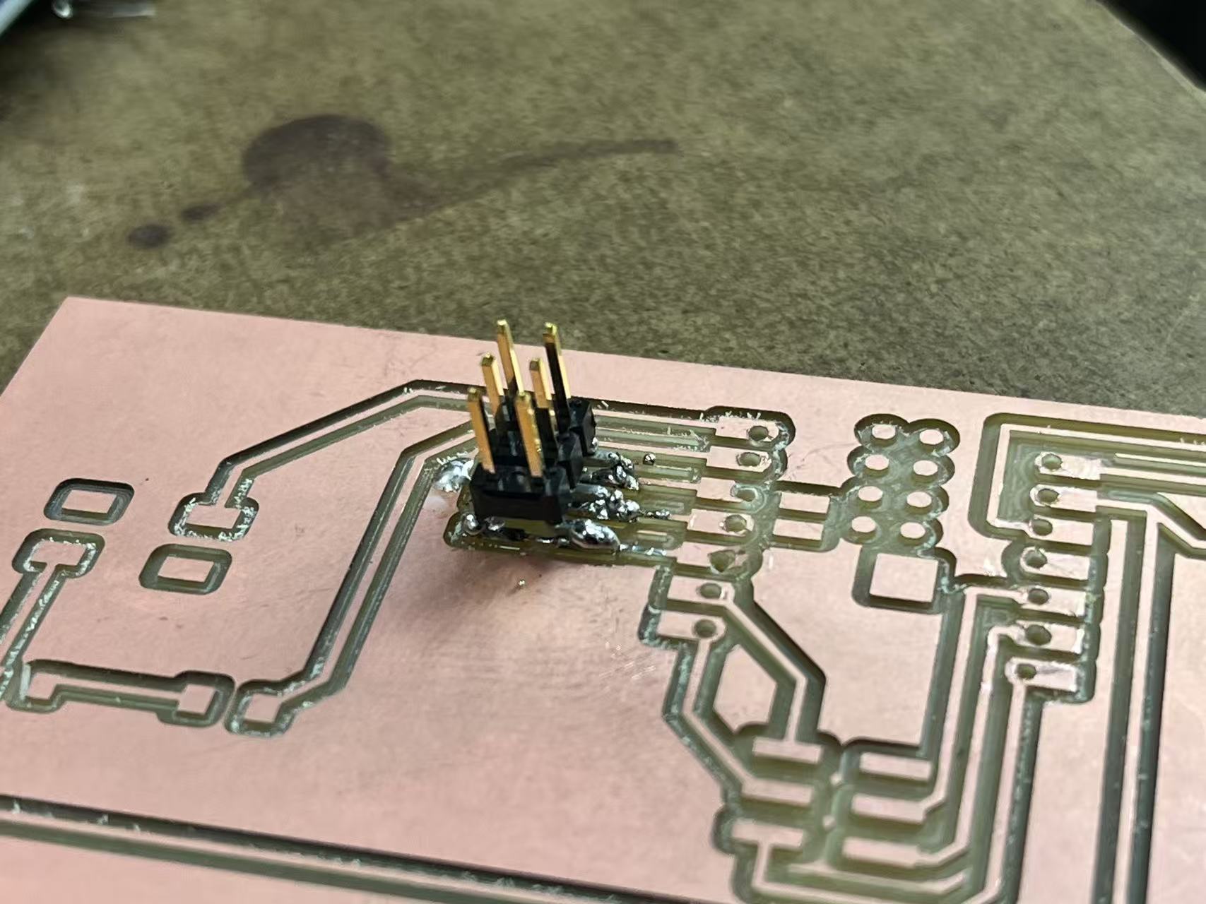
15. Soldering the first SMD components onto the freshly milled board.
More components populated on the board
16. Gradually populating passives, MCU, and connectors.
Finished soldering front side
17. Front side mostly finished, ready for power-up tests.
Board connected to power supply and USB
18. First power-on over bench supply and USB—watching for smoke and voltage drops.
LEDs lighting up
19. Status LEDs confirm that power rails and reset are behaving correctly.
Board connected to computer
20. Final check: board enumerates over USB/UART and responds to a simple test program.

Notes

Stable recipe on our mill: 1/64″ for traces at shallow DOC with a new bit; 1/32″ for outlines; vacuum + brush mid-cut to reduce shorts from dust; IPA wipe after milling; quick continuity check before soldering. Most of my early failures were about Z-height and worn tools, not the design itself.