Lap Timer
Electronics Production Project
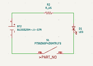
Board Design
This week is a continuation of lap timer project from last week, moving from design to production. I started by refining the board schematic and layout (cleaning up traces and adding mounting holes). I also corrected the input logic on the ESP32, which had been reversed.
The final board design, shown below, was used for milling and assembly.
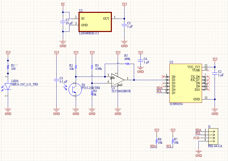
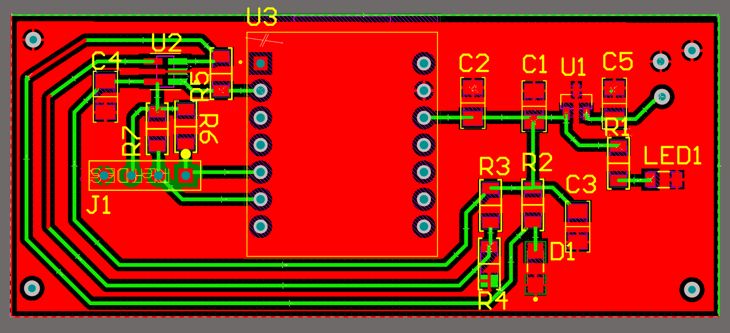
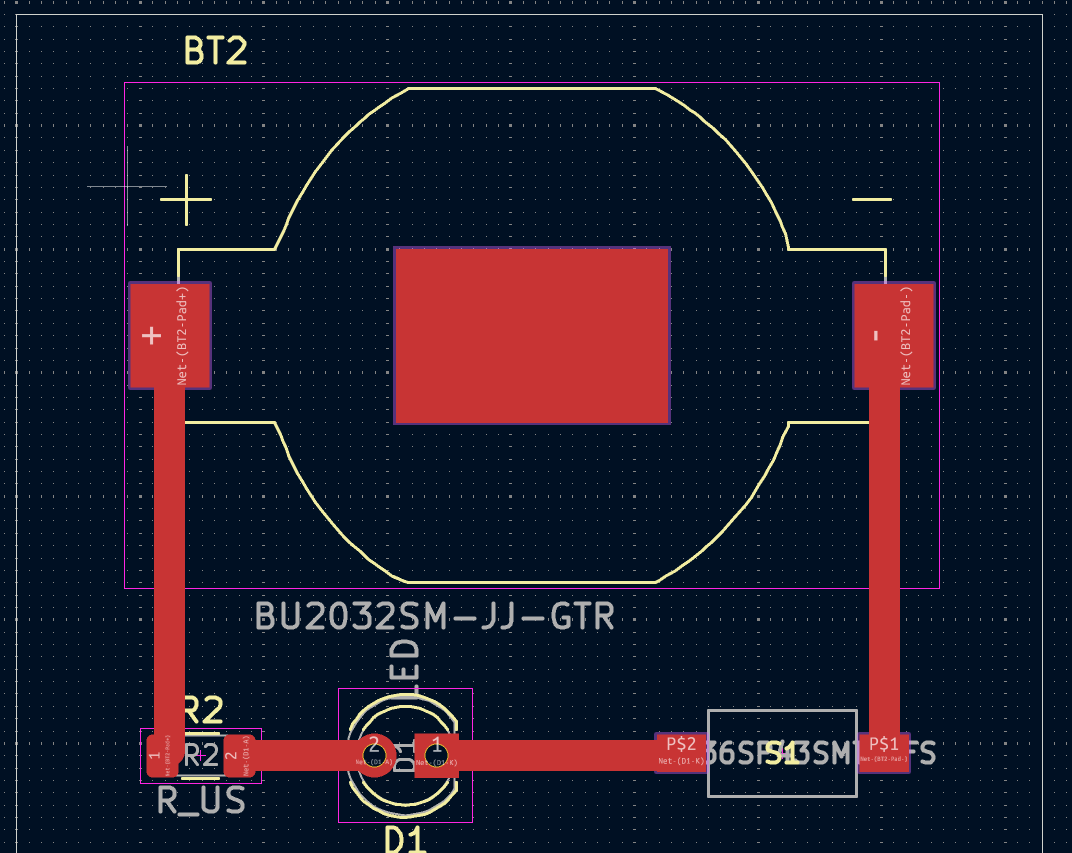
Layout
Milling
I milled the board using the Roland SRM-20 in the Architecture shop.
The goal was to cut the copper traces cleanly, drill through holes and mounting holes, then outline the board for removal.
I followed the protocol discussed in our required lab session and the Architecture shop milling tutorial.
I also found this Aalto Fablab Youtube video helpful for milling the through holes.
Steps:
- Prepare files
- Export the .png traces, holes and outline from Altium
- Use modsproject.org → Programs → Open Server Program → PCB → Roland SRM-20 → mill traces (1/64).
- Set the cut depth to 0.004 in and tool diameter to 0.0156 in (1/64 in) for traces.
- For the outline, switch to mill outline (1/32) and set depth to 0.012 in.
- Set up the machine
- Take the FR-1 board down firmly on the sacrificial bed using double-sided tape, pressing evenly so it's flat.
- Mount the 1.64 in end mill in the collet.
- In VPanel, set the XY origin at the lower-left corner of the board.
- Lower the Z until the bit barely touches the copper surface. Loosen the screw slightly, press it slightly into the surface, and then tighten again.
- Mill the traces
- Load the traces file in Mods and send the job to the mill.
- Watch the first few passes to make sure the copper is being cut away cleanly (not just scratched) and that the bit isn't cutting too deep.
- Use Pause and Resume in VPanel (DO NOT UNPLUG THE USB).
- Change tools for the drilling
- After milling the traces, raise the Z and switch to the 0.1 in. end mill.
- Re-zeo the Z in the same way.
- Switch to the through hole file in Mods and send the job.
- Change tools for the outline
- After milling the through holes, raise the Z and switch to the 1/32 in. end mill.
- Re-zero the Z in the same way.
- Switch to the outline file in Mods and send the job.
- Remove and Clean the Board
- Carefully pry the board off with a spatula.
- Clean of the tape residue with isopropyl alcohol.
- After Milling
- Check each pad under the microscope to make sure there's no leftover debris from milling.
- Check continuity between all connected pads using multimeter.
- Use deburring tool to smooth board edges.
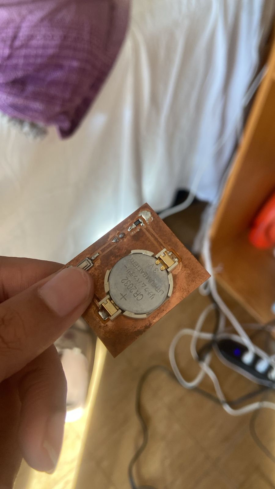
Soldering
After milling and cleaning the PCB, the next step was soldering all of the components onto the board.
I used the soldering iron in the Architecture shop with Pb-free solder following the instructions discussed in our required lab session and this Architecture shop soldering tutorial.
Steps:
- Organize components
- Stick all components onto a strip of double-sided take so they don't roll away or get lost.
- Label each part with its reference (e.g., R1, U1) so that it is easy to find while soldering
- Set soldering station temperature
- For most parts, I set the temperature to 350°C
- A few components, like the IR LED and photosensor, included solder temperature profiles in their datasheets. I adjusted the soldering temperature when soldering those components to ensure that I don't go above their reflow peak (point where splder melts and creates the necessary connection without exceeding the maximum temperature ratings of the component).
- Apply flux to pads
- Flux helps the solder to "wet" the pad and component leads by cleaning oxidation and improving surface tension.
- Plack and tack one side of the surface mounted component using tweezers
- Apply a tiny bit of solder to one pad on your PCB.
- Hold the surface mounted component with tweezers and position it over that pad
- Rehead the same pad with soldering iron while gently pressing the component into place. The solder will melt and hold that one side down.
- Verify that all polarity sensitive parts (LEDS, phototransistors) are oriented correctly.
- Reflow the other side by heating the opposite pad and applying a small amount of solder.
- Keep the soldering tip tinned and clean to avoid dull joints.
- If a joint looks frosty, reflow it with flux because it's likely oxidized.
- Avoid reheading the same pad multiple times
- Inspect each connection under the microscope after soldering. The solder joint should resemble the one in the image below:
- After Soldering
- Clean the board using isopropyl alcohol and soft brush to remove leftover flux reside.
- Check for bridges used multimeter.
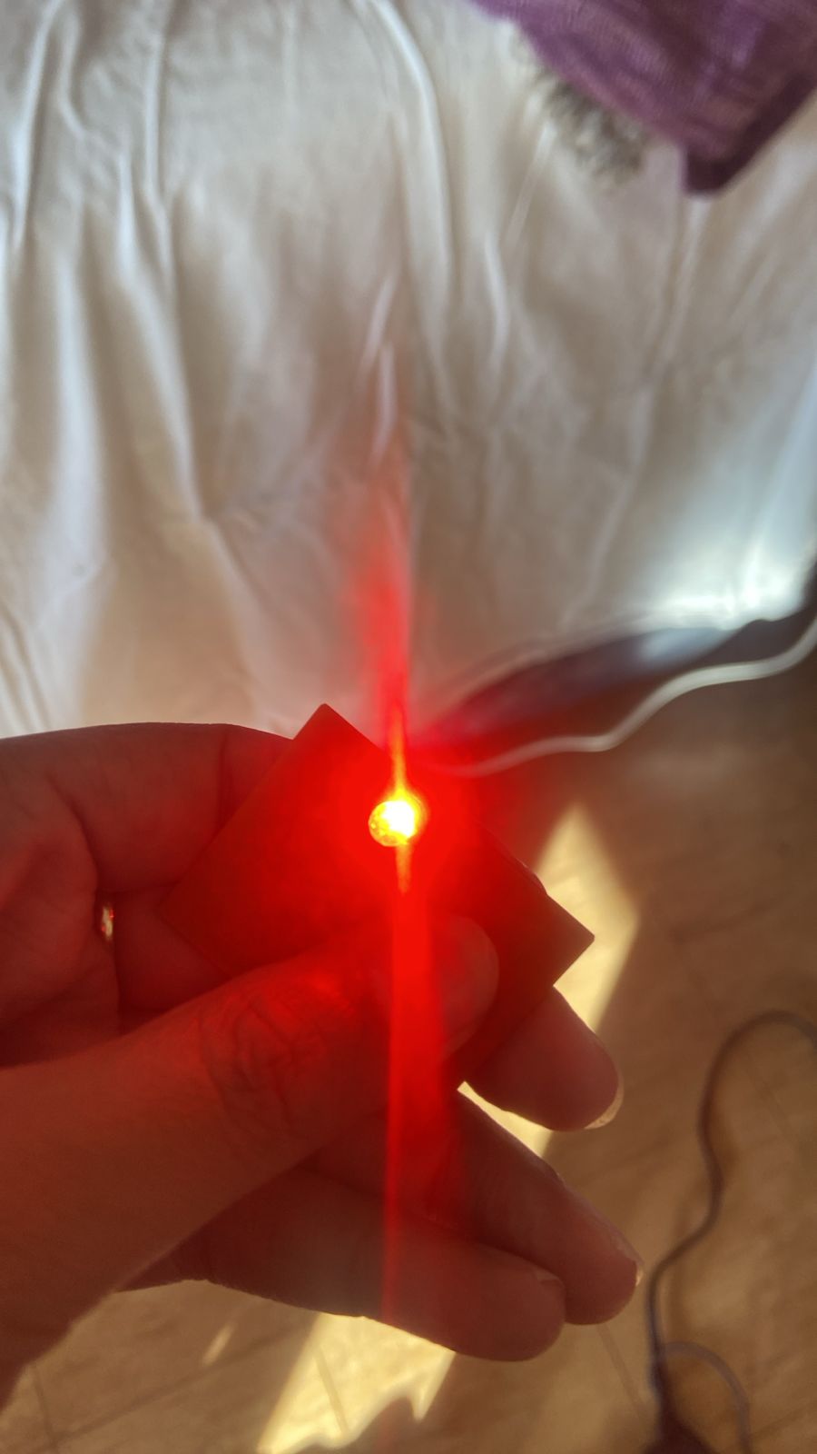
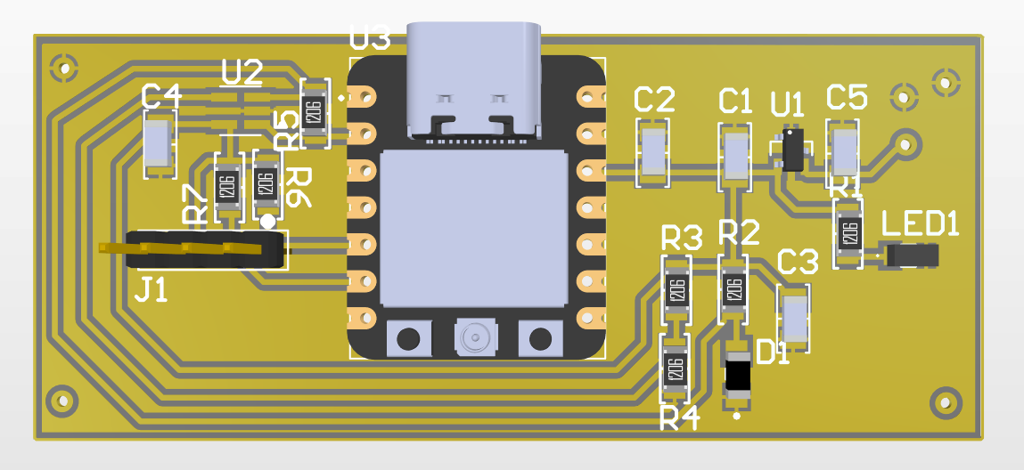
Final Product