Design My First PCB
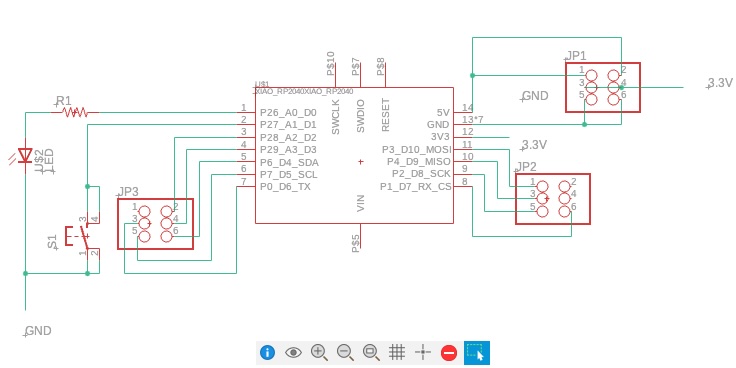
This week involved less hands-on work than previous weeks, but we covered crucial PCB design fundamentals. The process consists of two key steps: creating a schematic to show component relationships, and designing a PCB diagram to show how components connect on the actual board. The process became crystal clear thanks to a comprehensive video walkthrough by Anthony.
After about an hour of following the video instructions, I successfully created my first PCB design.
Practical Tricks When a Trace is Blocked
One of the most useful takeaways from the design process was learning workarounds when routing traces encounter obstacles. Here are three practical techniques:
Via jumpers — add a via to jump to the other side of the board, pass the obstacle, and via back to continue the trace.
0 Ω resistors — on single-layer boards, place a 0 Ω resistor so one net can "jump" over another without crossing.
Temporary keepouts — draw a route keepout corridor before placing copper pours to reserve space for critical traces.
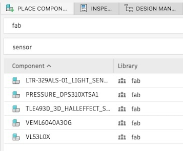
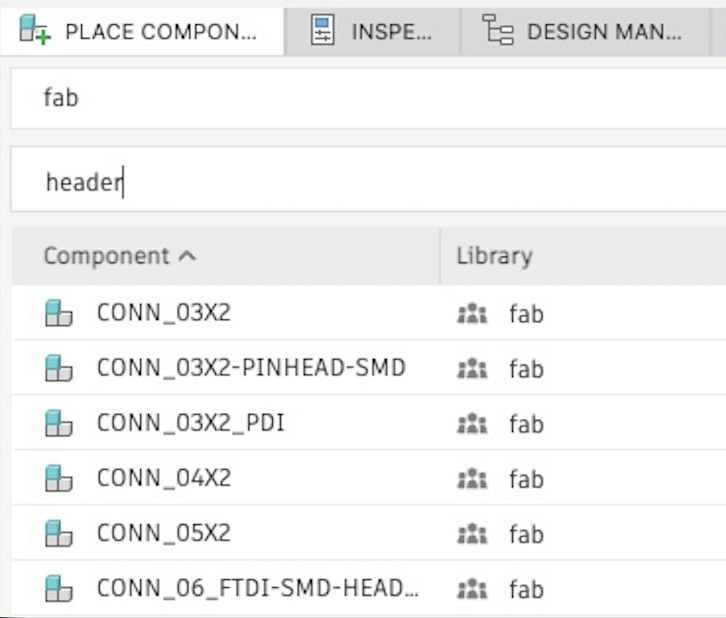
Component Library Overview
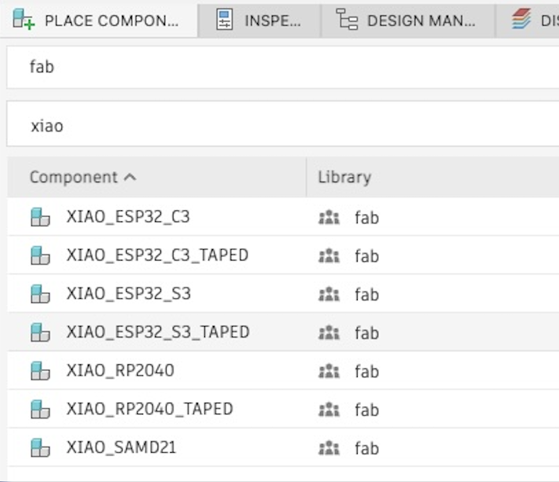
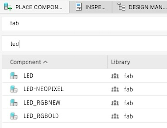
The fab library offers a wide variety of components we can use. Here are some key parts available:
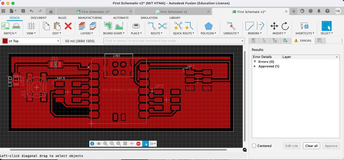
PCB Design Ready for Fabrication