Assignment
-
group assignment:
- send a message between two projects
-
individual assignment:
- design, build, and connect wired or wireless node(s)
- with network or bus addresses and local input &/or output device(s)
What to make
For my final project I will have multiple secondary MCU that talks to the main MCU via I2C. For this week, I want to build one of the secondary MCU that connects to a PS2 device and send the data to the main MCU via I2C. The connection between the secondary MCU and the main MCU is wired, and will connected through JST-XH 2.54mm pitch 4-pin connector.
Research
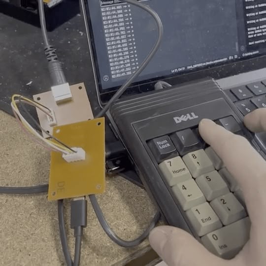
I started by searching for a past project that uses a PS2 device and interprets the data with an Arduino board. djsadeepa posted one such project on Instructables.
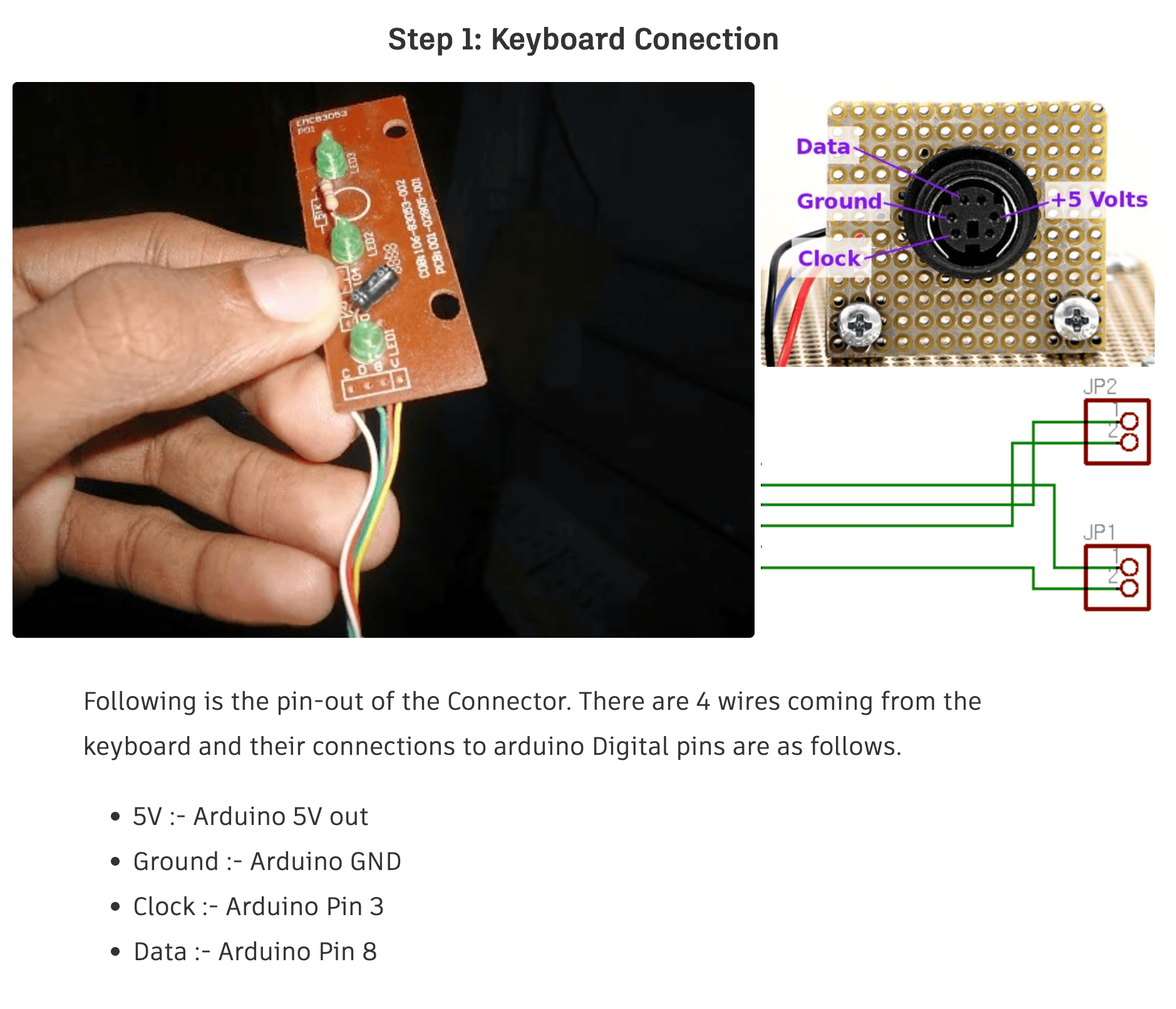
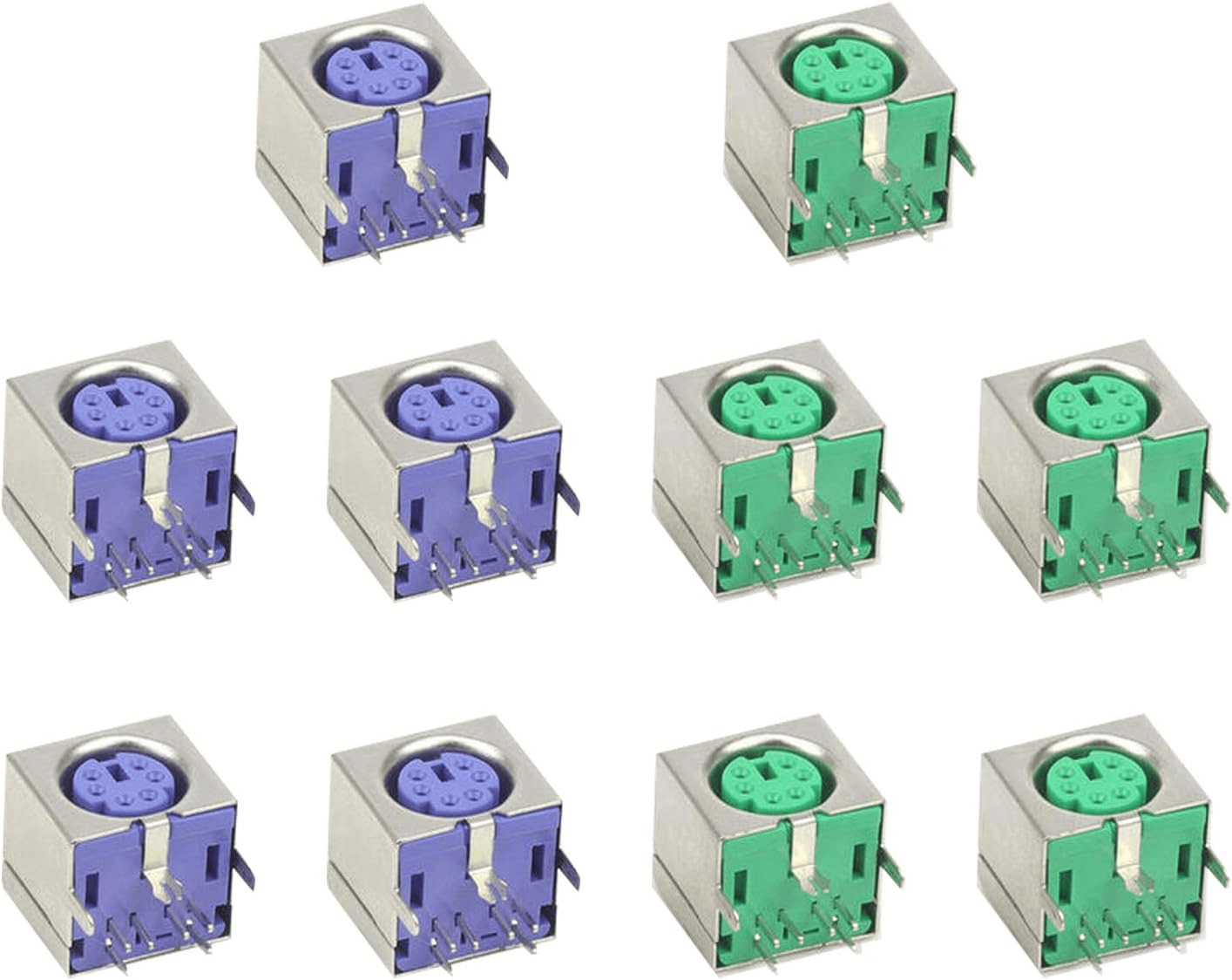
I turns out that for a PS/2 device using the mini DIN 6-pin connector, there are only 4 pins that are used for data transmission: CLK, DATA, +5V, and GND. All I need to do is to connect the CLK and DATA pins to the microcontroller and the rest will happen in software.
PS/2 Port
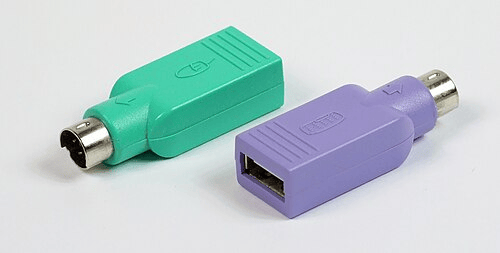
I read a bit more into the PS/2 protocol on Wikipedia. I was always fascinated by the "interoperability" of the PS/2 protocol with USB, remembering these passive USB adapters. I always thought it's a backward compatibility feature from USB, but turns out to be that the I/O device would have to support both protocols, and the adapter only swap the wires to make it fit.
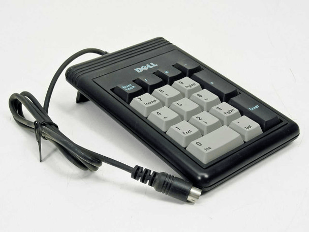
I bought a cute little PS/2 numpad from ebay, an Dell 86004 External Keypad PS/2 17 Key Numpad. It's hard to find a PS/2 numpad online, and this looks quite vintage. I'm not sure which year it was made.
To connect the numpad to the microcontroller, I bought a connector on Amazon to connect the numpad to the PCB.
PS/2 Connector Submodule
Since I plan to use the final product with another microcontroller, I want this to be its standalone submodule. The submodule will have:
- a microcontroller (XIAO ESP32 C3)
- a PS/2 port (to connect to the numpad)
- a JST-XH 2.54mm pitch 4-pin connector (to connect to the main MCU)
- also because I bought a kit from Amazon
Symbols & Footprints for PS/2 Port
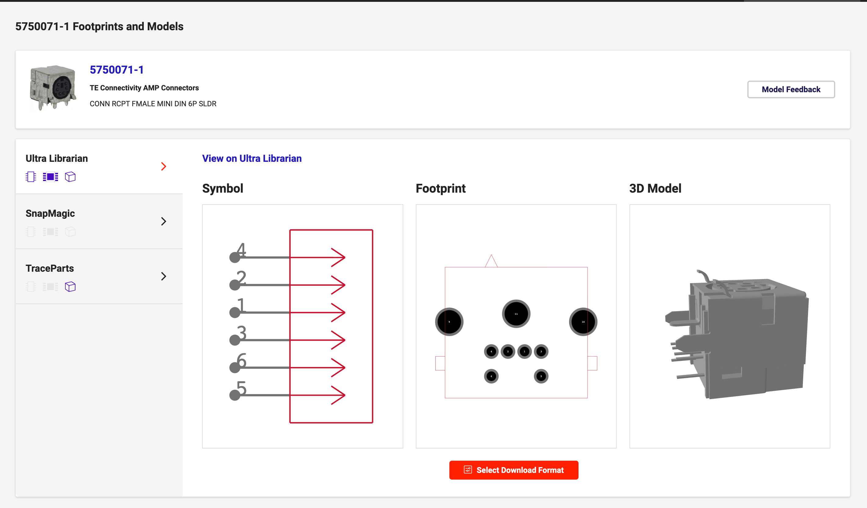
Searching for mini-DIN 6-pin connector, I couldn't find a symbol for my noname amazon connector. The closest I found is 5750071-1 from TE Connectivity AMP Connectors. I assumed it's the same as the connector I bought since it's industry standard (I've seen plenty of them on motherboards and other devices).
Symbols & Footprints for JST-XH 2.54mm pitch 4-pin connector
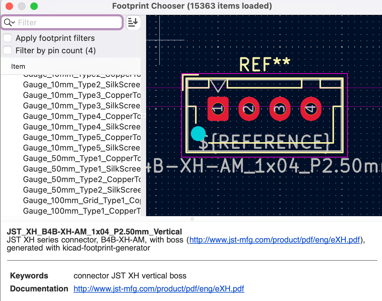
Although the HTMAA inventory includes symbols for JST connectors, the associated footprints did not match my XH series connector. I located the correct footprint in KiCad's connector library: Connector_JST:JST_XH_B4B-XH-AM_1x04_P2.50mm_Vertical.
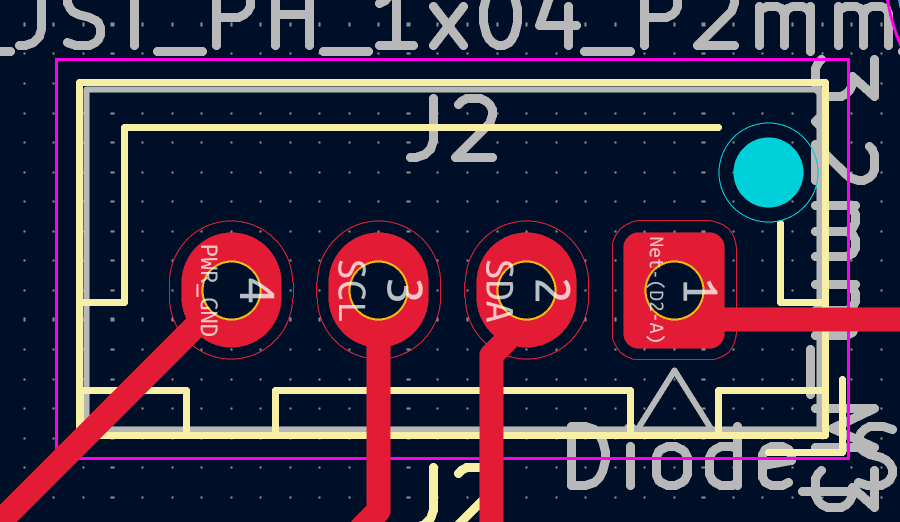
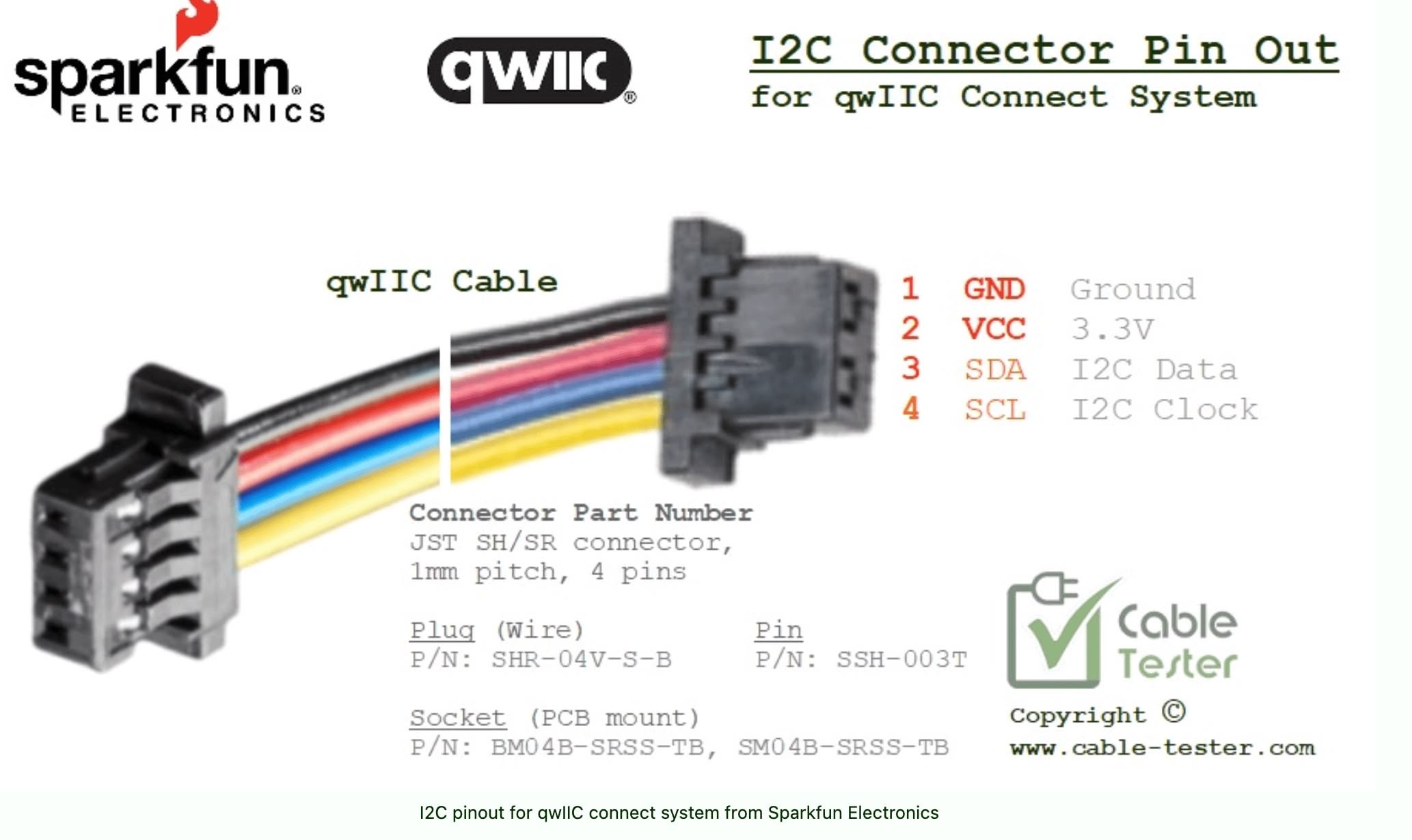
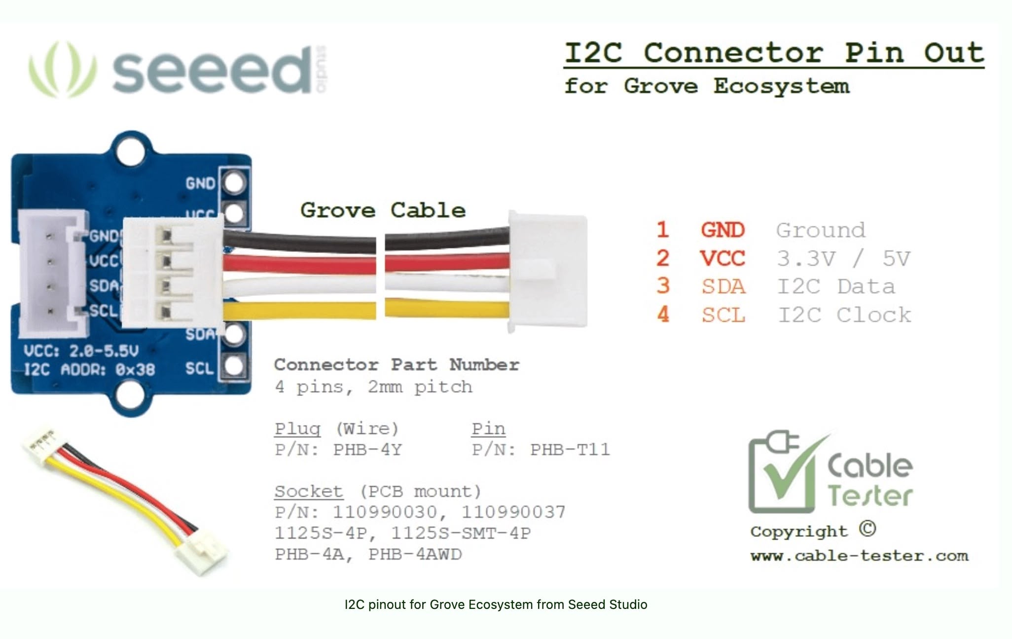
I used this 4-pin connector for I2C communication. One key difference in my design is the use of 5V power instead of the typical 3.3V, as the numpad requires 5V. My custom pinout configuration is VCC, SDA, SCL, and GND. Initially, I thought placing power and ground on opposite ends was a good practice for isolation. However, I later discovered that established ecosystems like Seeed's Grove and SparkFun's Qwiic place power and ground pins adjacent to each other.
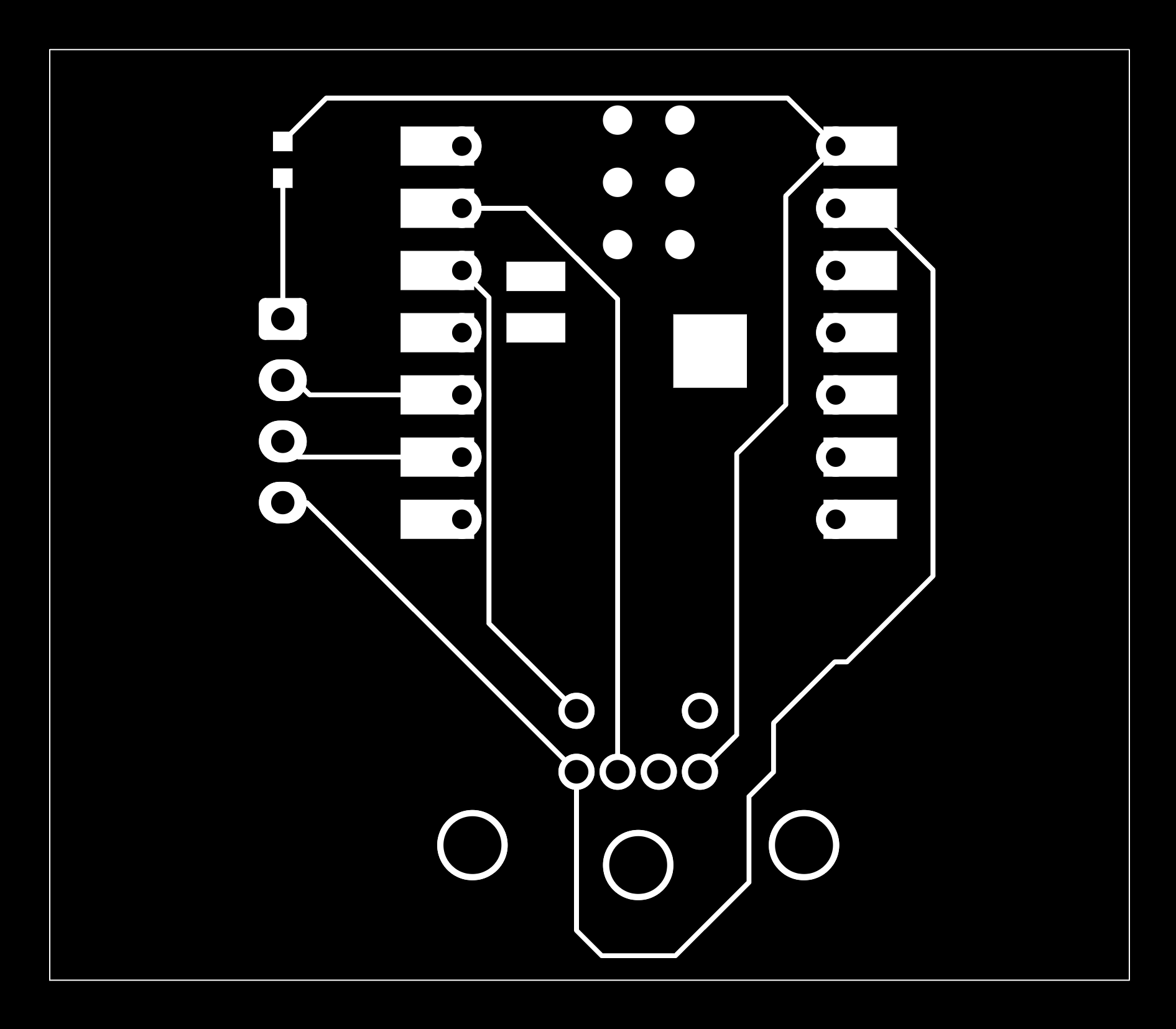
Schematics and PCB for Submodule
The schematic design is quite straightforward. I assigned GPIO 2 and GPIO 3 for SDA and SCL communication, respectively. I used GPIO 3 for PS/2 Data and GPIO 4 for PS/2 Clock. Additionally, I included a Schottky diode at the JST power input to indicate that this module serves as an input device and to prevent potential reverse power flow.
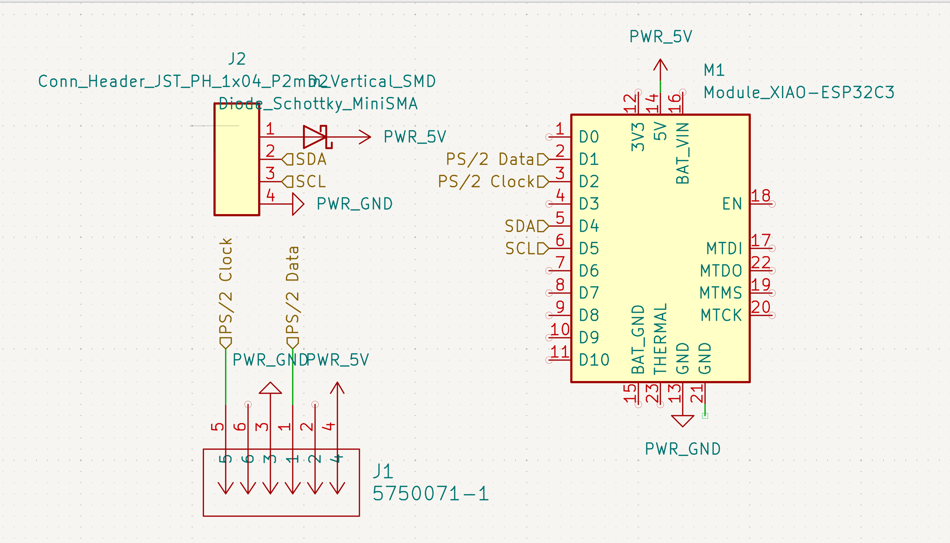
However, this design choice proved problematic. The diode introduced a voltage drop that compromised the power supply to the keyboard (for reasons I'll explain later). Consequently, I replaced the diode with a 0Ω resistor to resolve the issue and simplify the circuit.
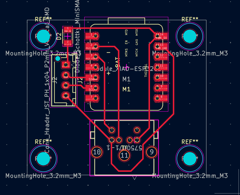
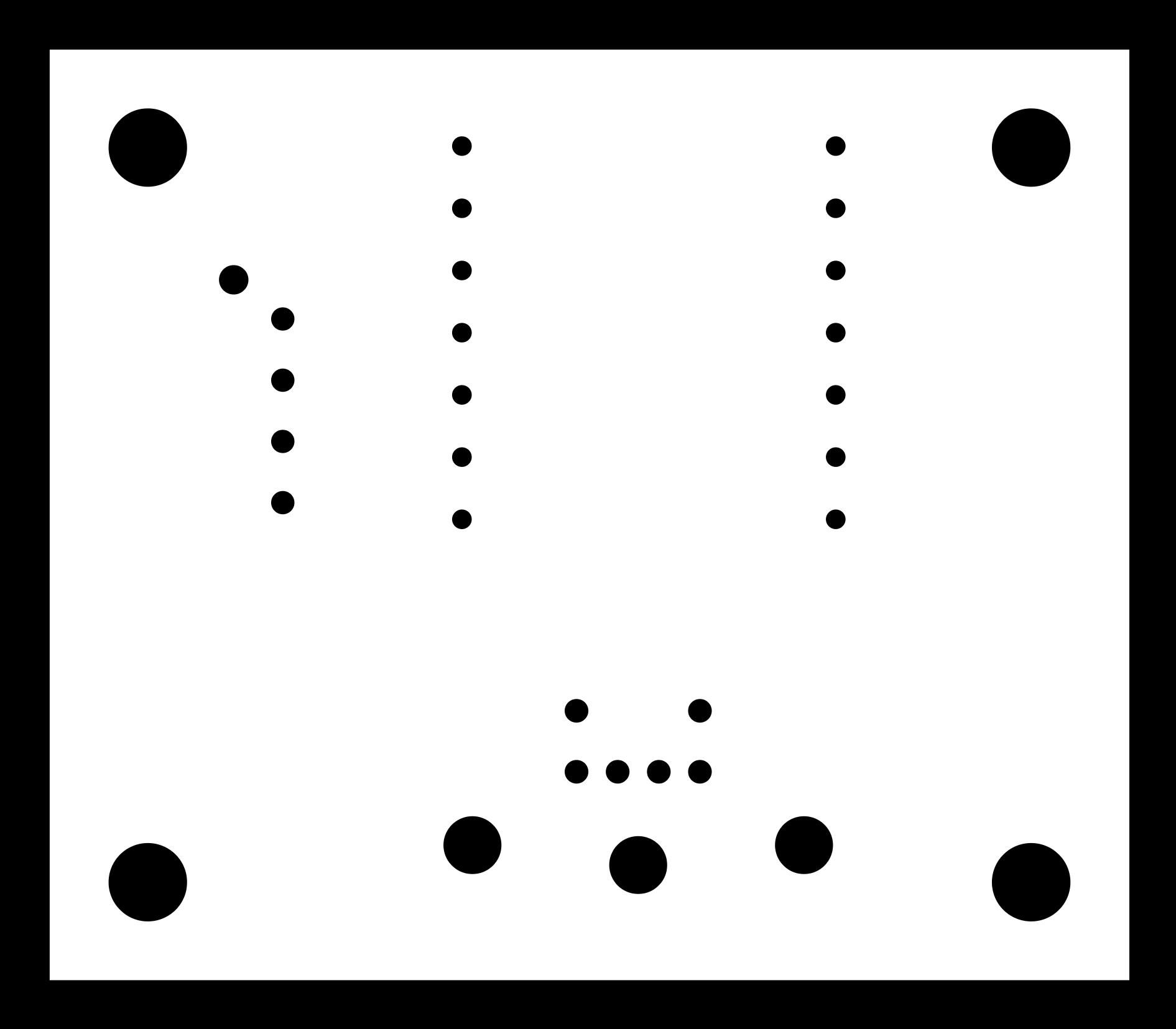
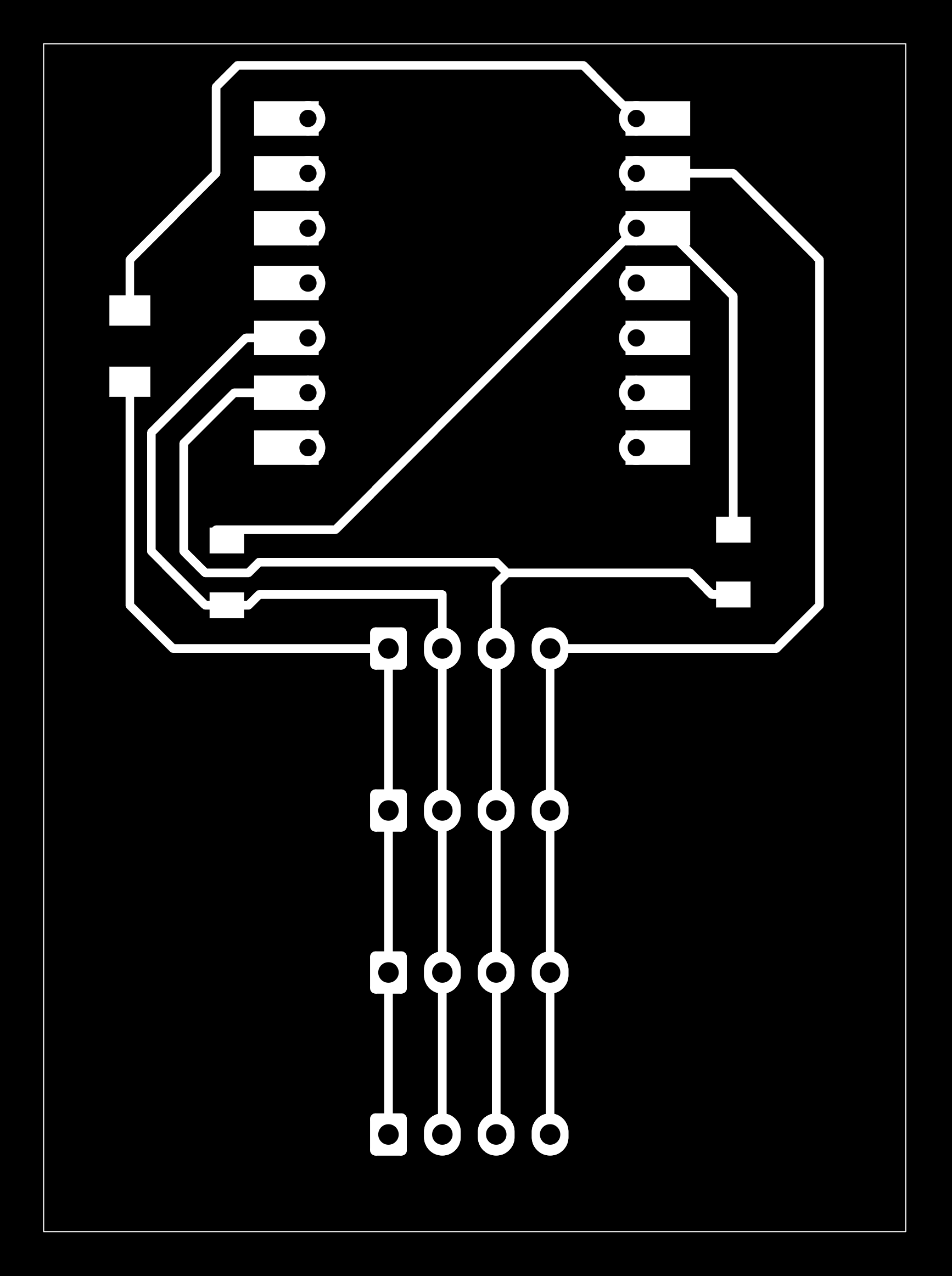
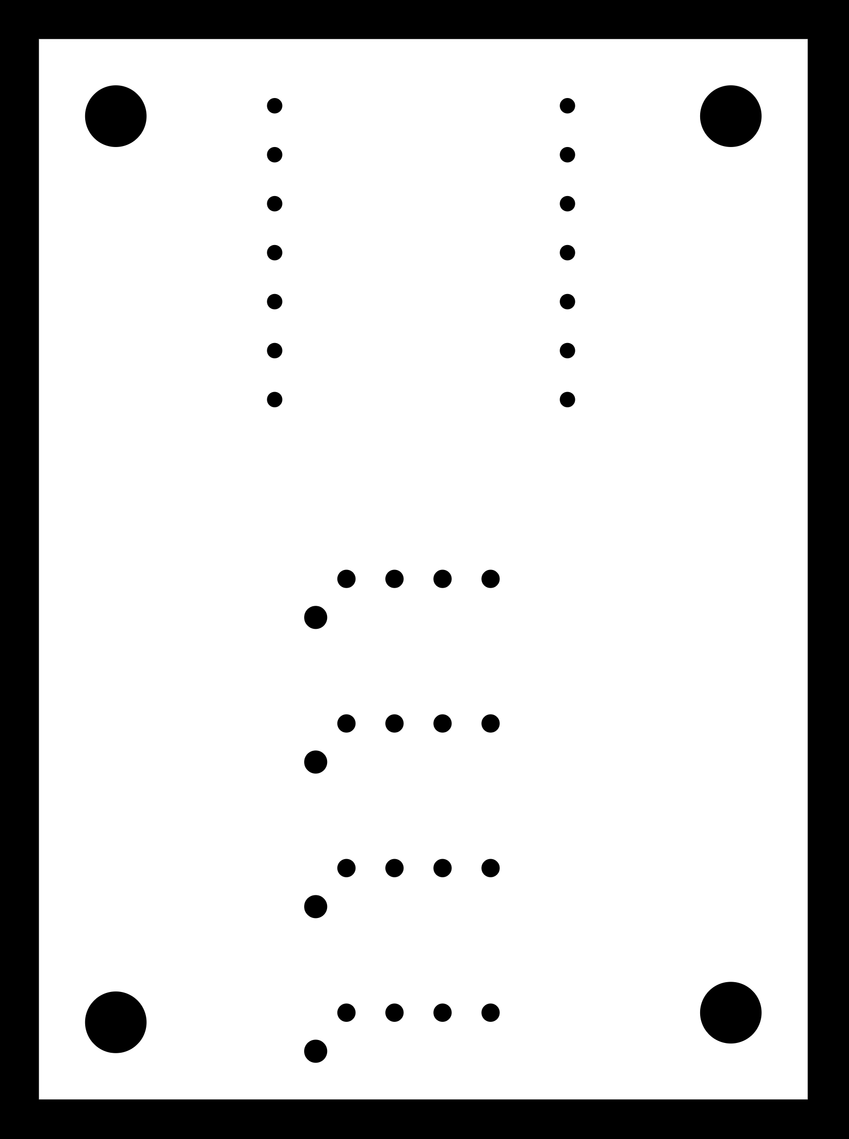
The PCB layout is similarly straightforward. I included four M3 mounting holes at the corners to facilitate easy installation. The routing prioritizes direct connections between the connector and the microcontroller, keeping the board compact and functional.
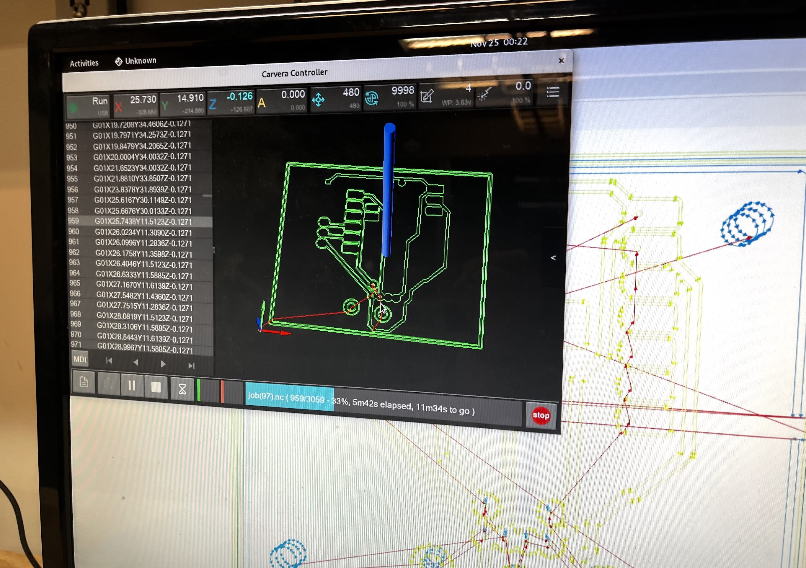
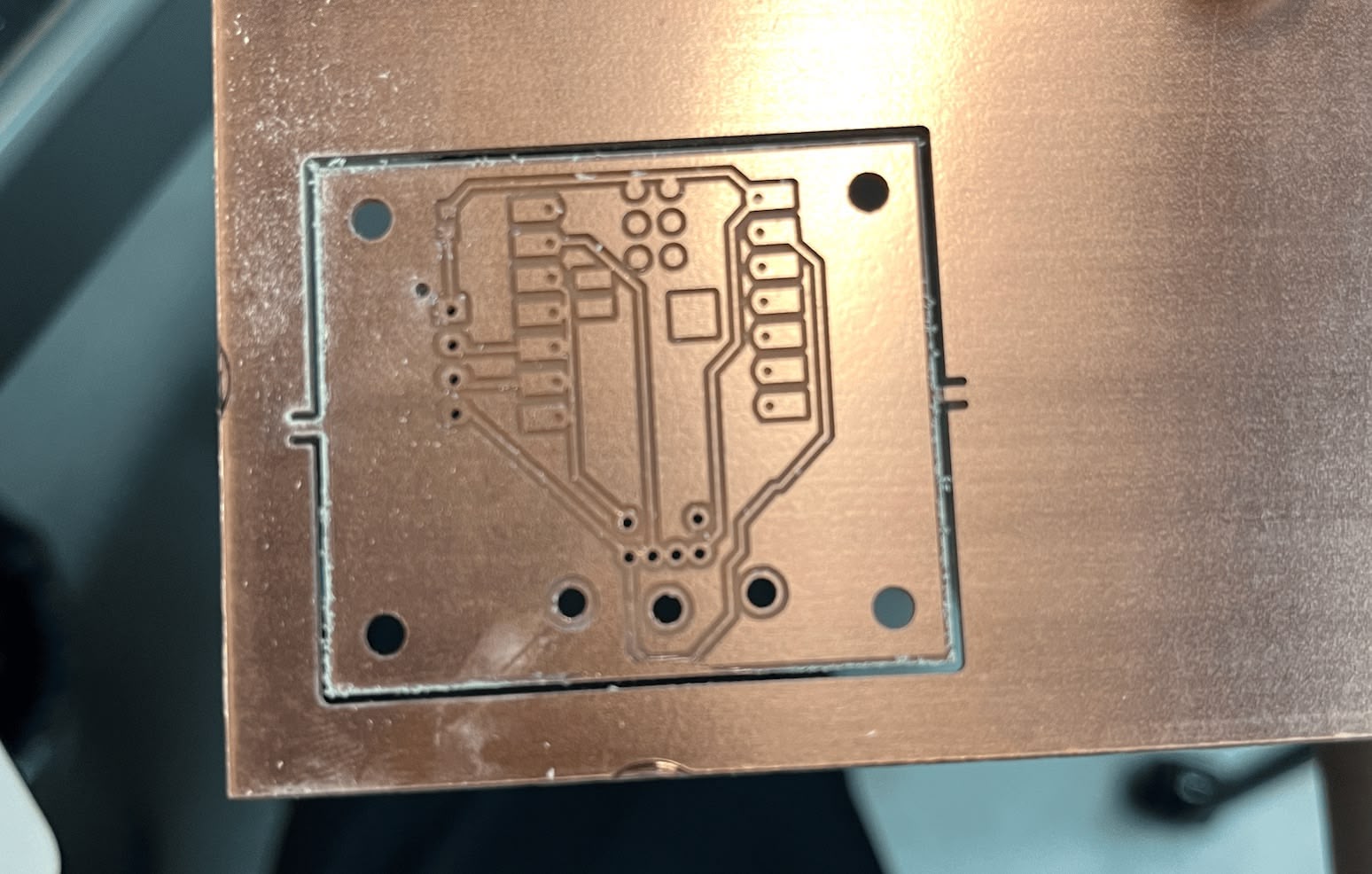
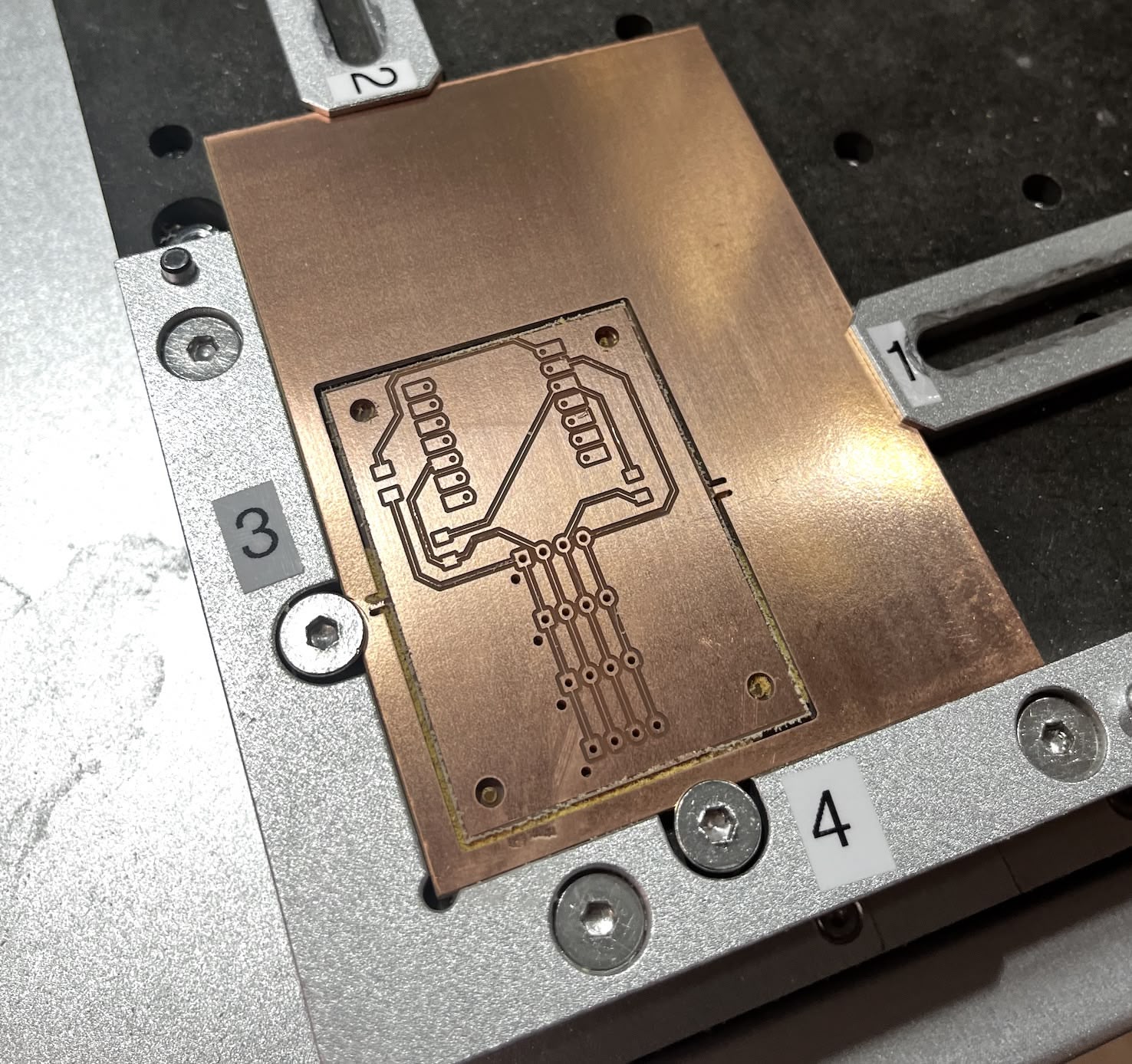
Milling Submodule PCB
To mill the PCB, I utilized the black and white images generated from the Gerber files using Gerber2Img, a tool made by Quentin Bolsée and Jake Read at the MIT Center for Bits and Atoms (2023). I then generated the toolpaths for the Carvera machine using Mods, a browser-based CAM tool.
Here is the milled PCB, fresh off the machine.
I did a test fitting with the PS/2 connector before soldering to ensure everything fits correctly.
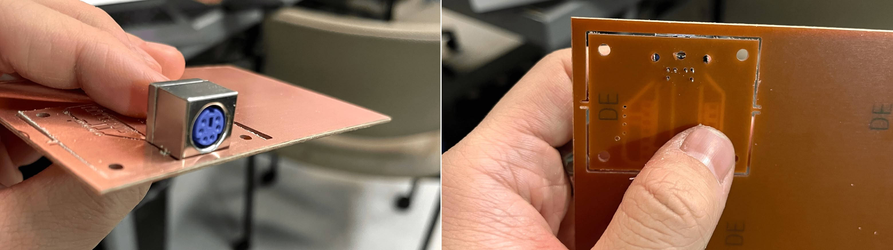
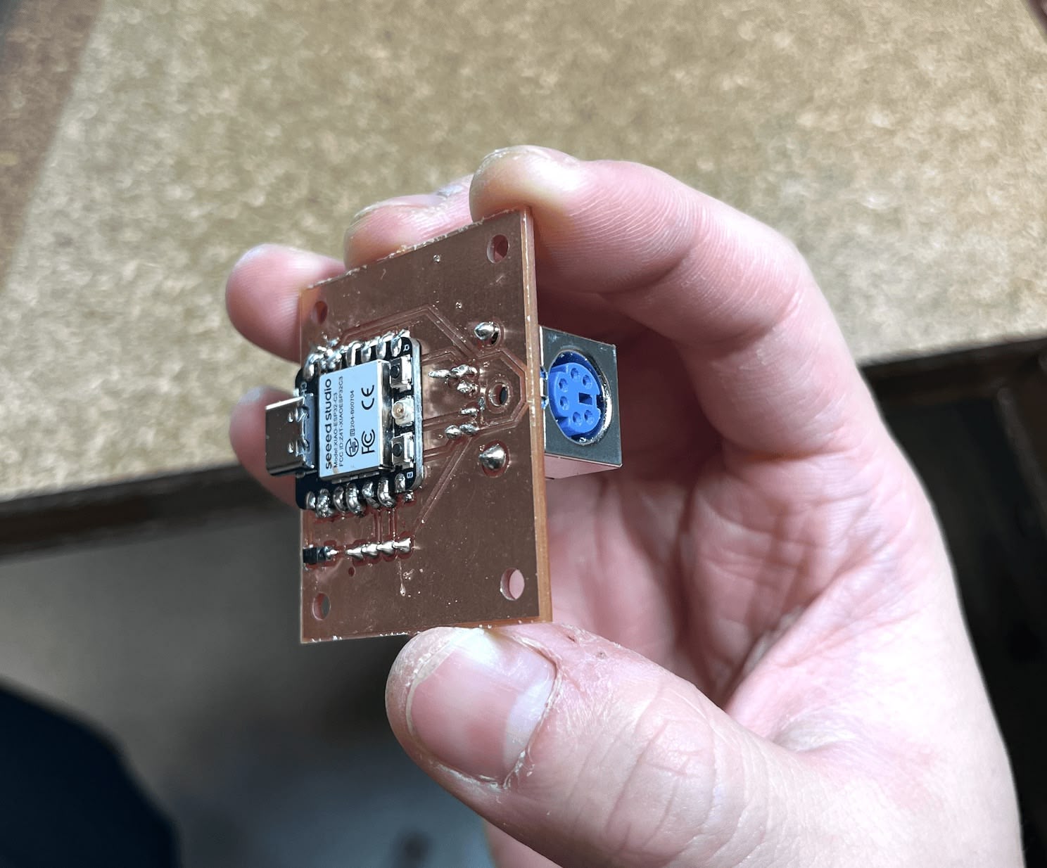
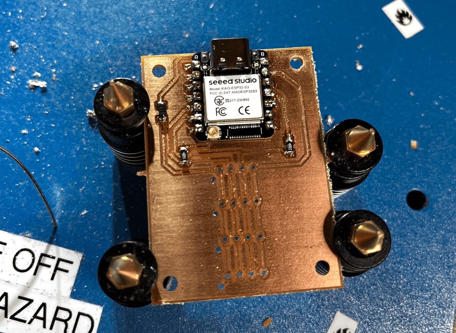
After soldering the components, including the XIAO ESP32 C3, the JST connector, and the PS/2 port, the submodule was ready.
Soldering Submodule PCB
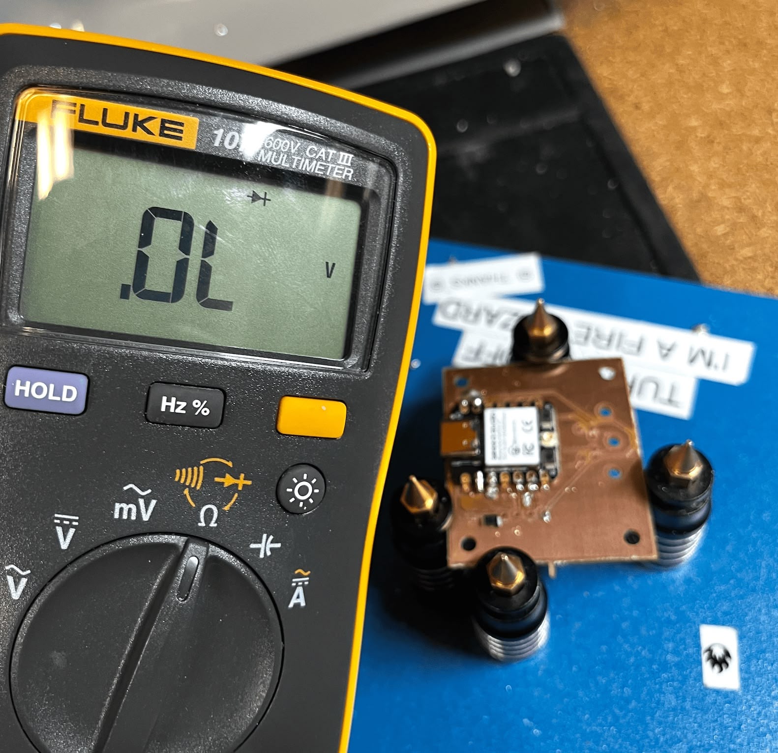
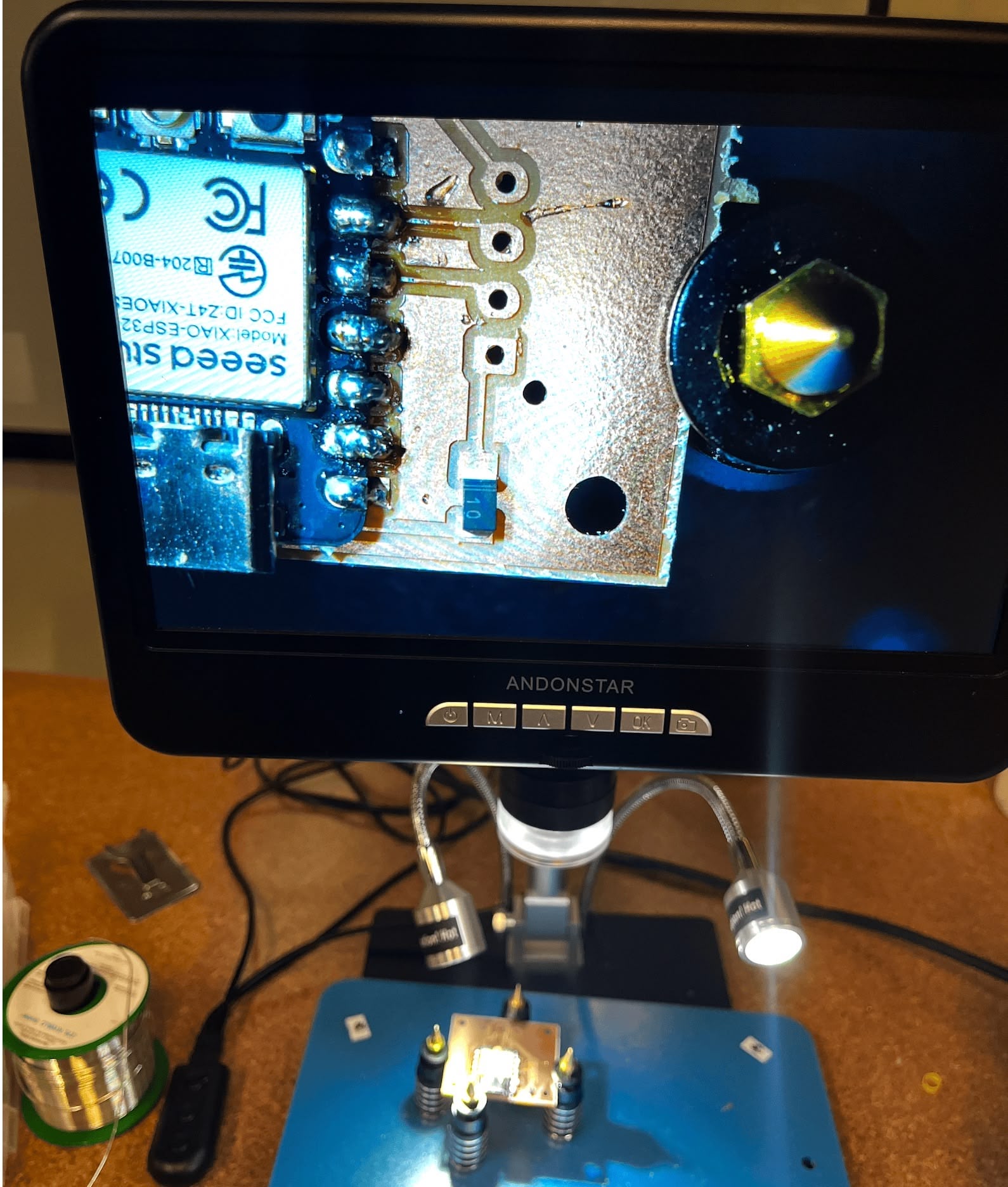
One tricky part was verifying the diode's directionality. The component is incredibly small, making it difficult to remember or even see the orientation markings. I had to use a multimeter to ensure it was placed correctly before soldering.
I also inspected the diode under a microscope. It became clear that the current flows from the side marked "0" to the side marked "1". Initially counterintuitive, I realized it makes sense if you think of it as electricity flowing "from 0 to 1".
After soldering the components, including the XIAO ESP32 C3, the JST connector, and the PS/2 port, the submodule was ready.
Making JST Cables
There are countless tutorials on YouTube about crimping JST connectors, and following many of them led me to failure. It's surprisingly easy to crimp at the wrong location or expose the wrong length of bare copper. I learned the hard way that you only need about 1-2mm of exposed copper for JST connectors, whereas Dupont connectors require more.
The best tutorial I found is this video. It saved me a lot of frustration.
I used a wire stripper and crimper from a kit I bought on Amazon, along with ribbon cables from the fab inventory.
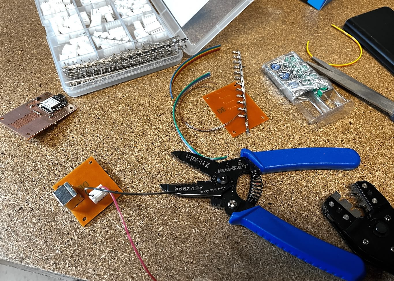
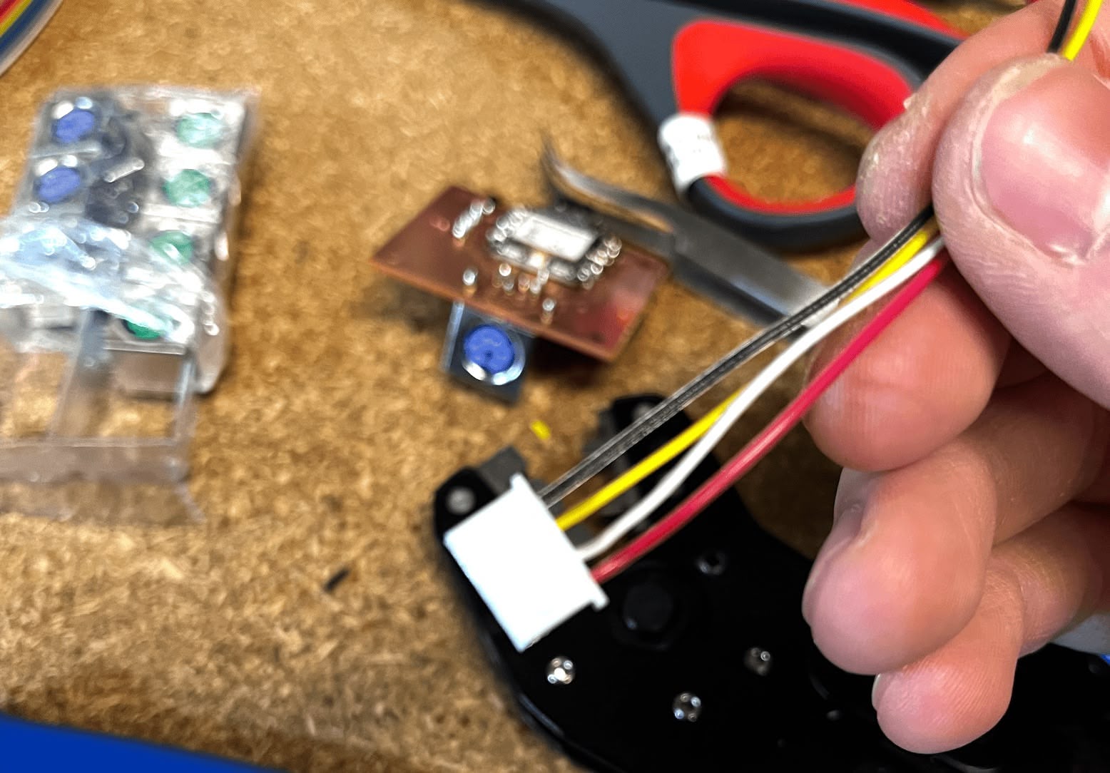
After crimping the pins onto the wires, I inserted them into the JST connector housing.
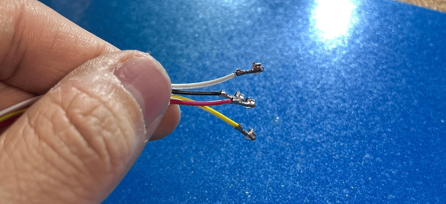
Here is the finished connector side with all four wires: red (5V), black (GND), yellow (Clock), and white (Data).
Voltage Drop Issues
After connecting the boards using the JST cables, I encountered an issue. The LED on the submodule board was only faintly lit. Upon testing with a multimeter, I found that the voltage had dropped to approximately 4.3V at the submodule.
This drop was caused by the diodes I included in the design for protection. There is one diode on the main board and another on the submodule, and each causes a voltage drop of roughly 0.3V. Since the PS/2 keyboard requires a 5V supply, this reduced voltage was insufficient for reliable operation.
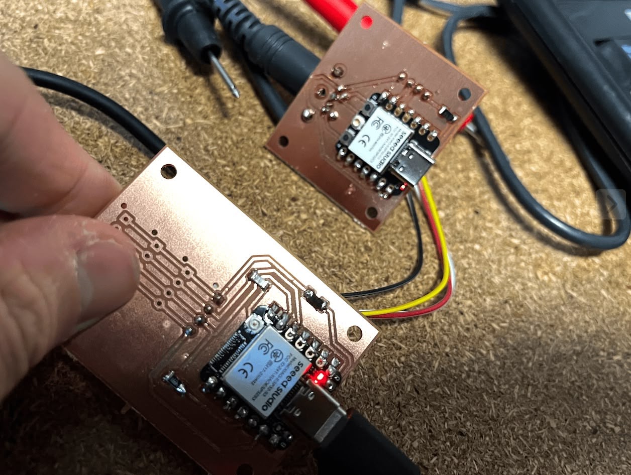
Realizing that I wouldn't be powering both boards simultaneously via USB-C in a way that would cause conflict, I decided to remove the protection diodes. I replaced the diodes on both the main board and the submodule with 0Ω resistors to restore the full 5V supply.
Main MCU Module
The main MCU module features an ESP32 S3 microcontroller, the same series as the XIAO ESP32 C3 but with expanded pinout capabilities. This board serves as the central hub, equipped with four JST-XH 2.54mm pitch 4-pin connectors. These connectors follow the same I2C pinout scheme (VCC, SDA, SCL, GND) with 5V power.
To ensure reliable I2C communication, I included 4.99kΩ pull-up resistors on the SDA and SCL lines, connecting them to the 3.3V rail. Each JST connector also has a designated slot for a diode, offering optional power protection.
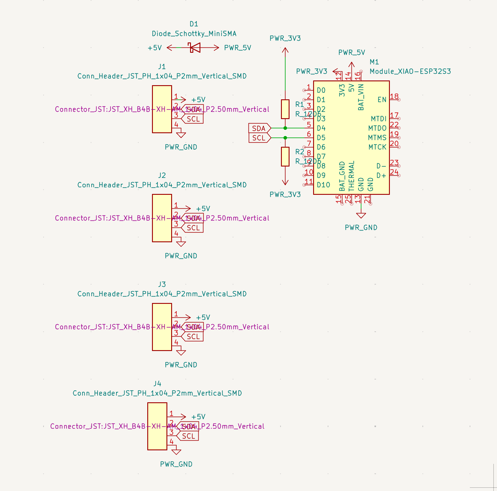
The PCB design accommodates these connectors and components while maintaining a logical flow for the I2C bus.
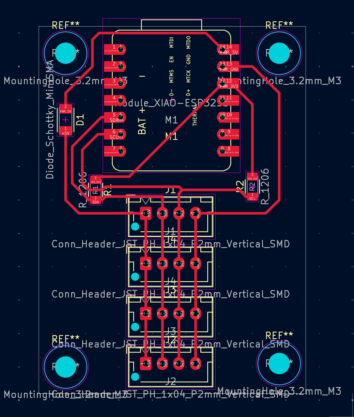
Milling Main MCU PCB
Similarly to the submodule PCB, I prepared the trace and edge cut images for milling.
Here is the result after milling:
I proceeded to solder the microcontroller, diodes, and pull-up resistors. (Note: I forgot to take a dedicated photo of the board with the JST connectors soldered at this stage, but you will see the fully assembled board in the following section).
Software Testing
Submodule Code
I started by testing the submodule independently to ensure the PS/2 keyboard could be read correctly. I used the PS2KeyAdvanced.h library developed by techpaul.
As seen in the video, the serial output displays hex codes (starting with 0x) which represent both press and release events. Most keys worked, though the '5' key was unresponsive. Despite this glitch, I proceeded with the implementation. I added a switch case in the code (shown below) to map these hex codes back to their corresponding ASCII characters.
Next, I implemented the I2C communication using the standard Arduino Wire.h library. The submodule is configured with a fixed I2C address of 0x08. The PS/2 Data pin is connected to GPIO 3, and the Clock pin to GPIO 4. The full code is available here.
#include <Wire.h>
#include <PS2KeyAdvanced.h>

#define PS2_DATA_PIN 3
#define PS2_CLK_PIN 4
#define I2C_SDA_PIN 6
#define I2C_SCL_PIN 7
#define I2C_ADDR 0x08

PS2KeyAdvanced keyboard;

#define BUFFER_SIZE 32
volatile uint8_t charBuffer[BUFFER_SIZE];
volatile uint8_t head = 0;
volatile uint8_t tail = 0;

void setup()
{
  Serial.begin(115200);
  keyboard.begin(PS2_DATA_PIN, PS2_CLK_PIN);
  Wire.begin(I2C_ADDR, I2C_SDA_PIN, I2C_SCL_PIN, 100000);
  Wire.onRequest(requestEvent);
  Serial.println("=== Smart Numpad Slave Ready ===");
}

void loop()
{
  if (keyboard.available())
  {
    uint16_t code = keyboard.read();

    // DEBUG: Print the raw code to see what's happening
    Serial.printf("Raw code: 0x%04X\n", code);

    // Ignore key releases (bit 15 set)
    if (code & 0x8000)
    {
      Serial.println("  -> Ignoring (release)");
      return;
    }

    // Extract just the key code (low byte)
    uint8_t keyCode = code & 0xFF;

    // Convert to ASCII
    uint8_t ascii = mapToAscii(keyCode);

    if (ascii != 0)
    {
      uint8_t nextHead = (head + 1) % BUFFER_SIZE;
      if (nextHead != tail)
      {
        charBuffer[head] = ascii;
        head = nextHead;
        Serial.printf("  -> Buffered: '%c' (ASCII 0x%02X from keyCode 0x%02X)\n",
                      ascii, ascii, keyCode);
      }
    }
    else
    {
      Serial.printf("  -> Not mapped (keyCode 0x%02X)\n", keyCode);
    }
  }
}

// THE CORRECT MAPPING based on PS2KeyAdvanced.h
uint8_t mapToAscii(uint8_t id)
{
  switch (id)
  {
  // Numpad (CORRECT codes from library)
  case 0x20:
    return '0'; // PS2_KEY_KP0
  case 0x21:
    return '1'; // PS2_KEY_KP1
  case 0x22:
    return '2'; // PS2_KEY_KP2
  case 0x23:
    return '3'; // PS2_KEY_KP3
  case 0x24:
    return '4'; // PS2_KEY_KP4
  case 0x25:
    return '5'; // PS2_KEY_KP5
  case 0x26:
    return '6'; // PS2_KEY_KP6
  case 0x27:
    return '7'; // PS2_KEY_KP7
  case 0x28:
    return '8'; // PS2_KEY_KP8
  case 0x29:
    return '9'; // PS2_KEY_KP9
  case 0x2A:
    return '.'; // PS2_KEY_KP_DOT
  case 0x2B:
    return '\n'; // PS2_KEY_KP_ENTER
  case 0x2C:
    return '+'; // PS2_KEY_KP_PLUS
  case 0x2D:
    return '-'; // PS2_KEY_KP_MINUS
  case 0x2E:
    return '*'; // PS2_KEY_KP_TIMES
  case 0x2F:
    return '/'; // PS2_KEY_KP_DIV

  // Regular numbers (top row)
  case 0x30:
    return '0'; // PS2_KEY_0
  case 0x31:
    return '1'; // PS2_KEY_1
  case 0x32:
    return '2'; // PS2_KEY_2
  case 0x33:
    return '3'; // PS2_KEY_3
  case 0x34:
    return '4'; // PS2_KEY_4
  case 0x35:
    return '5'; // PS2_KEY_5
  case 0x36:
    return '6'; // PS2_KEY_6
  case 0x37:
    return '7'; // PS2_KEY_7
  case 0x38:
    return '8'; // PS2_KEY_8
  case 0x39:
    return '9'; // PS2_KEY_9

  // Standard keys
  case 0x1C:
    return 8; // PS2_KEY_BS (Backspace)
  case 0x1E:
    return '\n'; // PS2_KEY_ENTER
  case 0x1B:
    return 27; // PS2_KEY_ESC
  case 0x1F:
    return ' '; // PS2_KEY_SPACE

  // Ignore lock keys themselves
  case 0x01:
    return 0; // PS2_KEY_NUM (NumLock key)
  case 0x02:
    return 0; // PS2_KEY_SCROLL
  case 0x03:
    return 0; // PS2_KEY_CAPS

  default:
    return 0; // Ignore
  }
}

void requestEvent()
{
  if (head != tail)
  {
    Wire.write(charBuffer[tail]);
    tail = (tail + 1) % BUFFER_SIZE;
  }
  else
  {
    Wire.write(0x00);
  }
}
Main MCU Code
I then tested the main MCU to ensure it could properly communicate with the submodule over I2C. Using the standard Arduino Wire.h library, I wrote code to scan for the submodule at address 0x08 and request data from it.
The code initializes the I2C bus and periodically polls the submodule for keystrokes. If a character is available, it is read and printed to the serial monitor.
#include <Wire.h>

#define I2C_ADDR 0x08
#define I2C_SDA_PIN 6
#define I2C_SCL_PIN 7

void setup()
{
  Serial.begin(115200);
  Wire.begin(I2C_SDA_PIN, I2C_SCL_PIN, 100000); // Master mode
  Serial.println("=== Main MCU Master Ready ===");
}

void loop()
{
  Wire.requestFrom(I2C_ADDR, 1); // Request 1 byte

  if (Wire.available())
  {
    char c = Wire.read();
    if (c != 0)
    {
      Serial.printf("Received: '%c' (0x%02X)\n", c, c);
    }
  }

  delay(50); // Small delay to avoid flooding
}
(Note: The actual code file for the mainboard is available here, but for clarity, I've simplified the explanation above to focus on the I2C interaction logic.)
Integration Test
Finally, I connected the USB-C cable to the main board, which in turn powered the submodule and established communication through my custom JST I2C connector. The integration was successful, with the main board correctly receiving keystrokes from the PS/2 numpad via the submodule.
References
- Components & Datasheets
- Tools & Fabrication
- Software & Libraries
- Research & Tutorials
