Assignment
- group assignment:
- characterize the design rules for your in-house PCB production process
- submit a PCB design to a board house
- individual assignment:
- make and test an embedded microcontroller system that you designed
- extra credit: make it with another process
From last week
Last week, I designed a PCB for the XIAO RP2040 and the PixArt PMW3360 sensor. This week, I'm fabricating it using the in-house milling machine.
Redesigning the PCB
The Gerber Export Problem
My first step was to export the Gerber files from my week 5 KiCad project. I followed the standard export procedure and uploaded the files to gerber2img, a tool that converts Gerber files to images for milling.
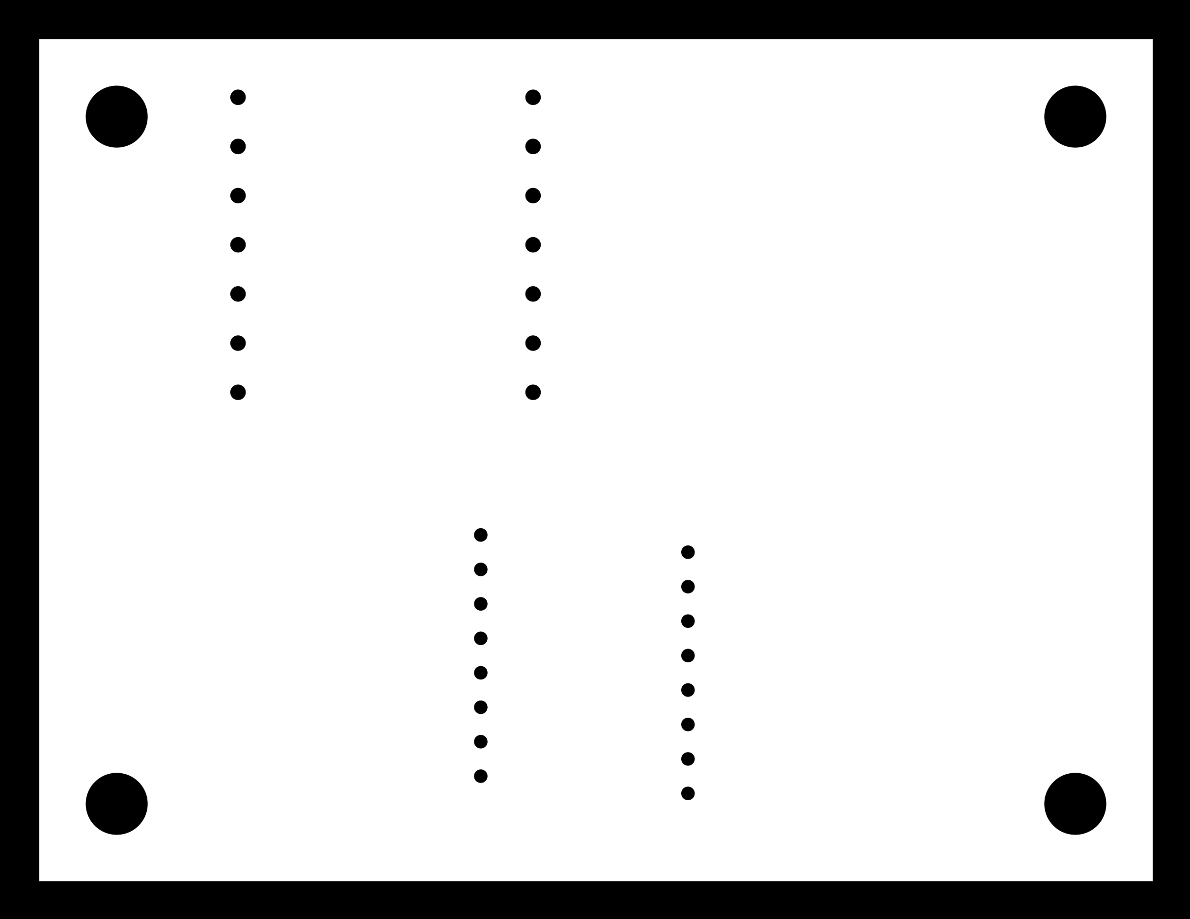
As you can see above, the exterior layer image from gerber2img does not show the expected cutout for the PMW3360 sensor, and the trace layer is completely empty—no copper traces at all. This indicated that gerber2img couldn’t interpret my week 5 Gerber files properly. After some debugging, I realized this might be because my week 5 project built directly on top of jfedor2's open source schematics, rather than starting from scratch. Some legacy settings or nonstandard layering likely caused these export issues.
Starting from Scratch
Rather than spending more time debugging, I decided to start fresh. This time, I would build the entire project from the ground up, ensuring clean exports.
PMW3360 Symbol and Footprint
For the PMW3360 sensor, I downloaded the symbol and footprint from SnapMagic. Last week, I had concerns about this footprint missing some pins, but I decided to give it another look.
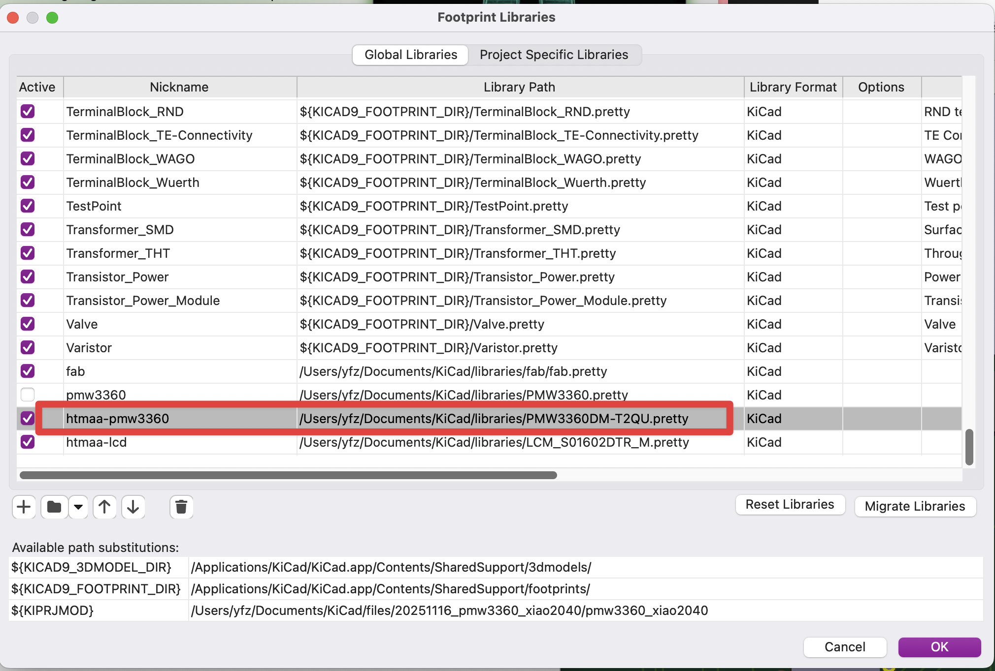
After importing them into KiCad and cross-referencing with the datasheet, the footprint appeared correct for my needs.
The Voltage Regulator Challenge
As discussed last week, the PMW3360 requires a 1.8V power supply, which isn't available in the fab lab inventory. I needed to source my own voltage regulator.
I found the AMS1117 series regulators on Amazon - a kit containing multiple voltage variants (1.2V, 1.5V, 1.8V, 2.5V, 3.3V, 5V) in SOT-223 packages. The AMS1117-1.8 would be perfect for stepping down the XIAO RP2040's 3.3V output to the required 1.8V for the sensor.
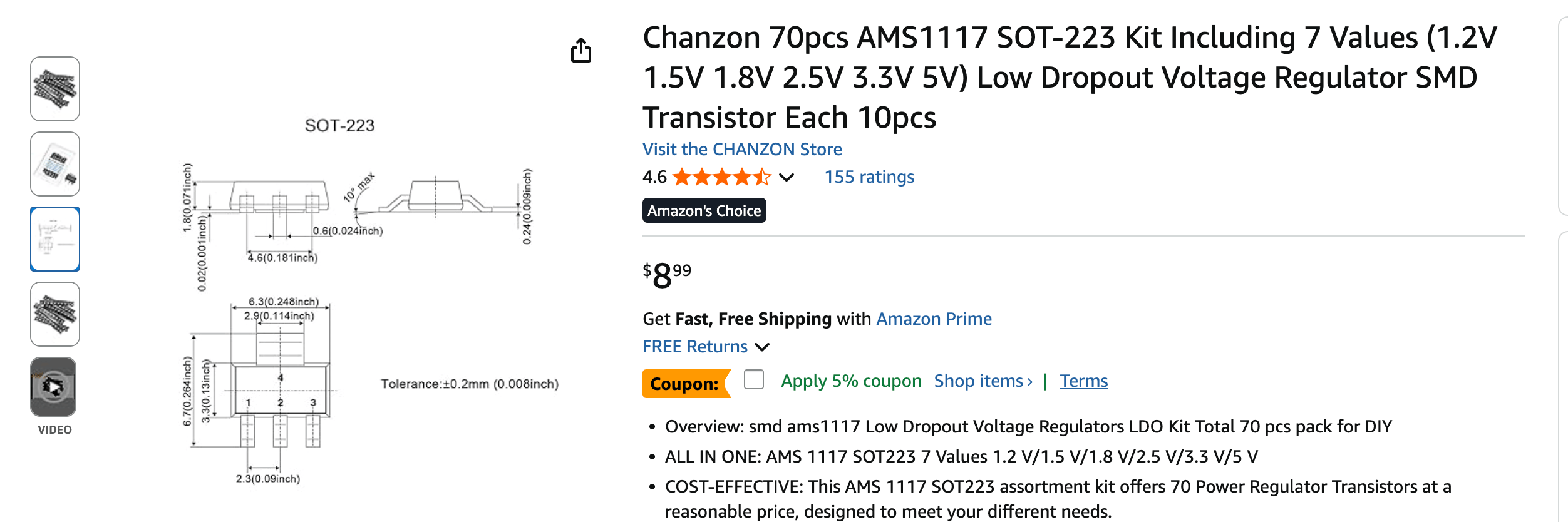
Fortunately, KiCad has the AMS1117 symbol and footprint in its default library, so I didn't need to create custom components.
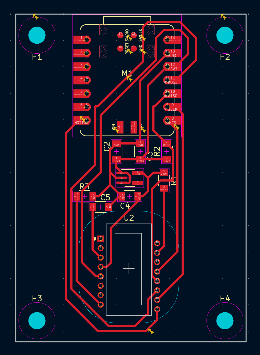
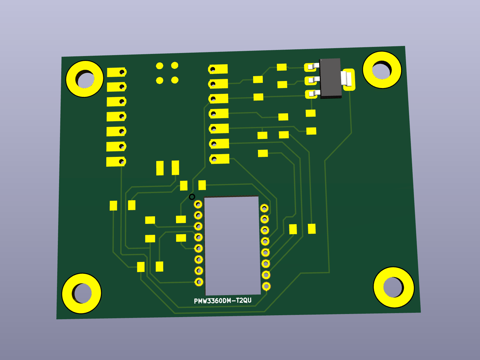
Schematics Design
Here's my final schematics for the PCB. The key components are:
- XIAO RP2040: The microcontroller board with SPI interface
- PMW3360: The optical sensor requiring SPI communication
- AMS1117-1.8: Voltage regulator stepping 3.3V down to 1.8V
- Capacitors: For power supply stability
- 0Ω Resistors: Used as jumpers for cleaner routing
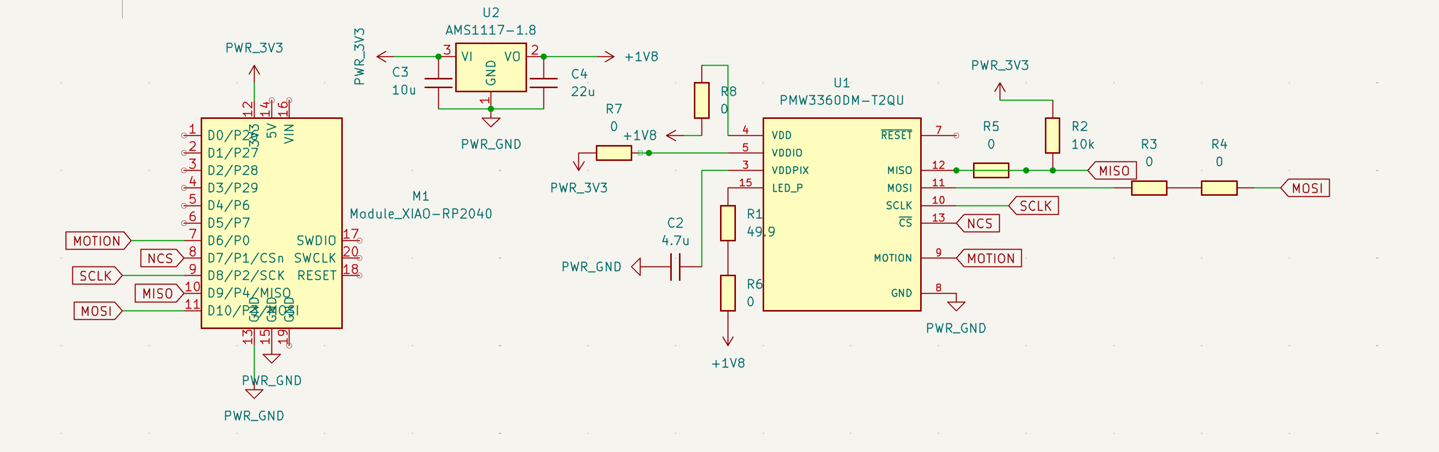
The main connections:
- SPI pins (MISO, MOSI, SCLK) connect the RP2040 to the PMW3360
- NCS (Not Chip Select) connects to a GPIO pin for software control
- 3.3V from XIAO feeds into the AMS1117 regulator
- 1.8V output from regulator powers the PMW3360
- Ground plane connects all components
PCB Layout Design
The 0Ω Resistor Strategy
One of my main goals this time was to create a cleaner routing topology. Last week's design had some convoluted paths due to the single-layer constraint. This time, I liberally used 0Ω resistors as jumpers to avoid routing conflicts.
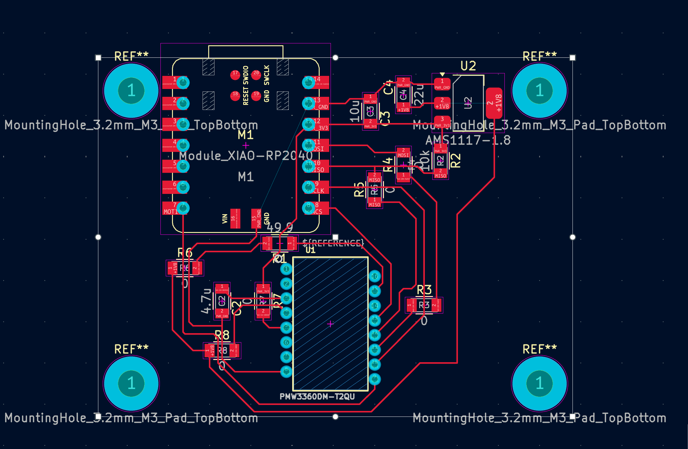
The 0Ω resistors act as bridges, allowing traces to "jump over" each other on a single-layer board. While this adds more components to solder, it makes the routing much more manageable.
The Cutout Under the Sensor
The PMW3360 is an optical sensor that needs a clear view of the surface below it. This requires a rectangular cutout in the PCB directly underneath the sensor's optical window.
Fabrication
Gerber Export
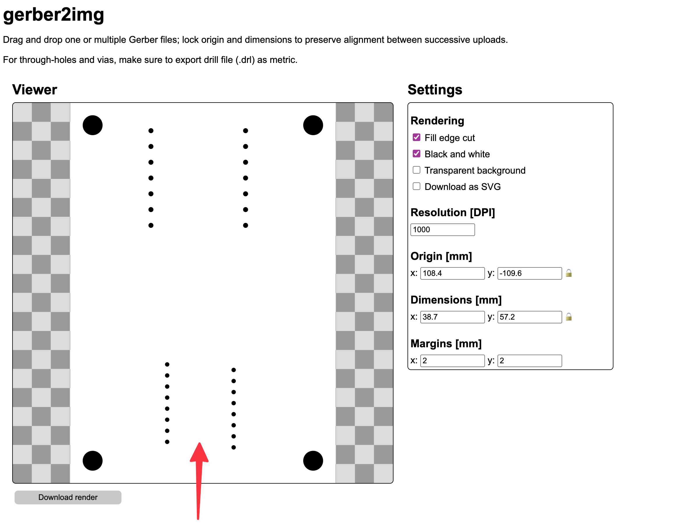
With the new design complete, I exported the Gerber files again and uploaded them to gerber2img.
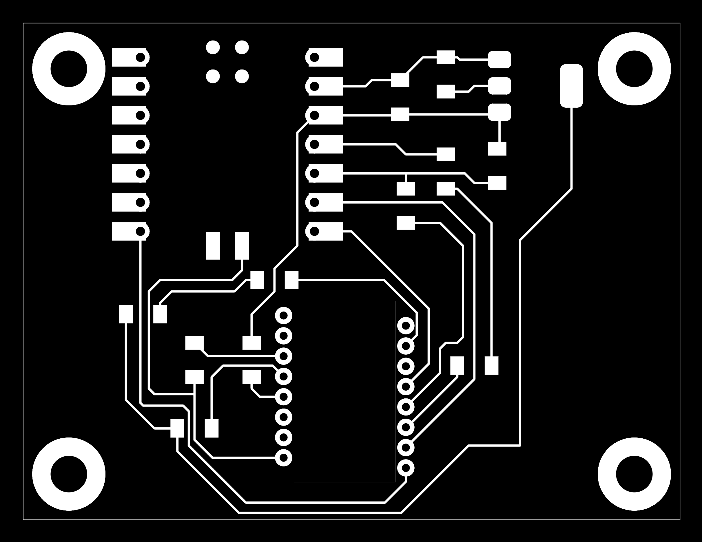
Much better! The traces, pads, and drill holes all appeared correctly... except for one thing.
The Missing Cutout
When I checked the "edge cut" layer image, the rectangular cutout under the PMW3360 sensor was still not showing up. But you've seen the 3D view in KiCad, which rendered the cutout perfectly. This suggested the issue was with the gerber2img tool's interpretation, not my footprint or PCB design.
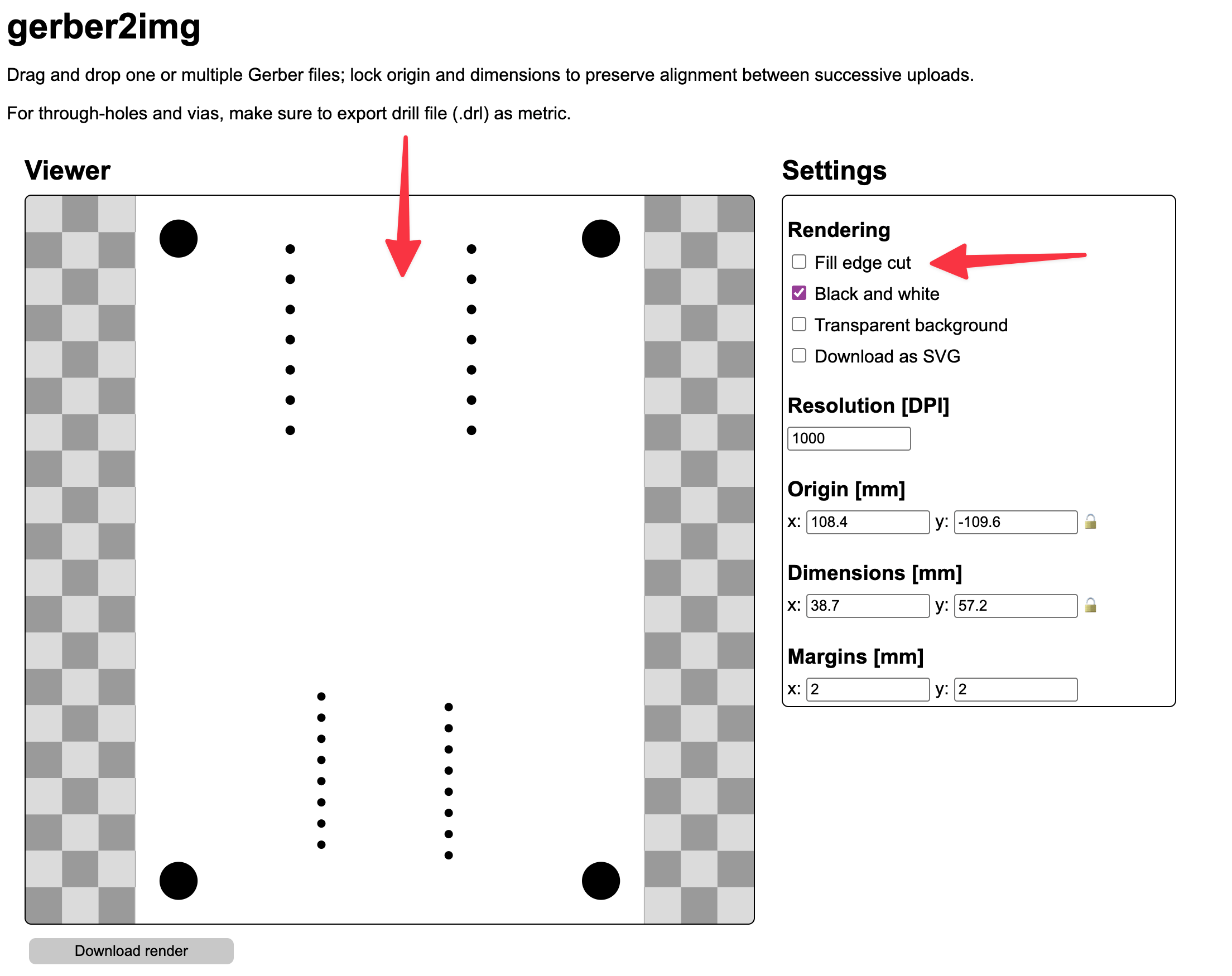
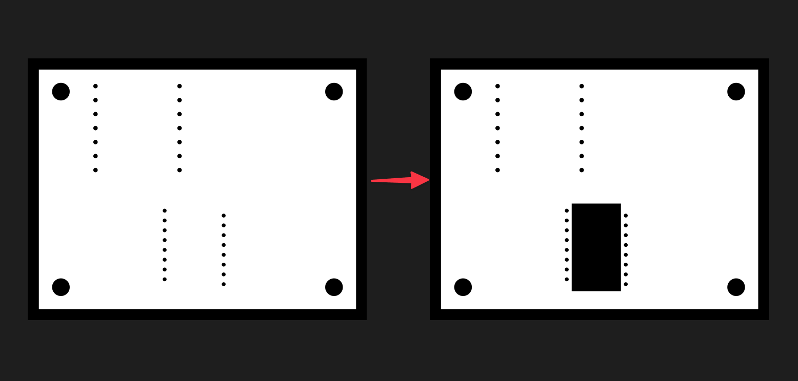
The Photoshop Workaround
Rather than diving into debugging the tool, I decided on a practical workaround. I exported the edge cut image from gerber2img, opened it in Photoshop, and manually added a black-filled rectangle where the cutout should be.
Generating Toolpaths with Mods
With the corrected images ready, I used mods to generate the toolpaths for the Carvera CNC mill.
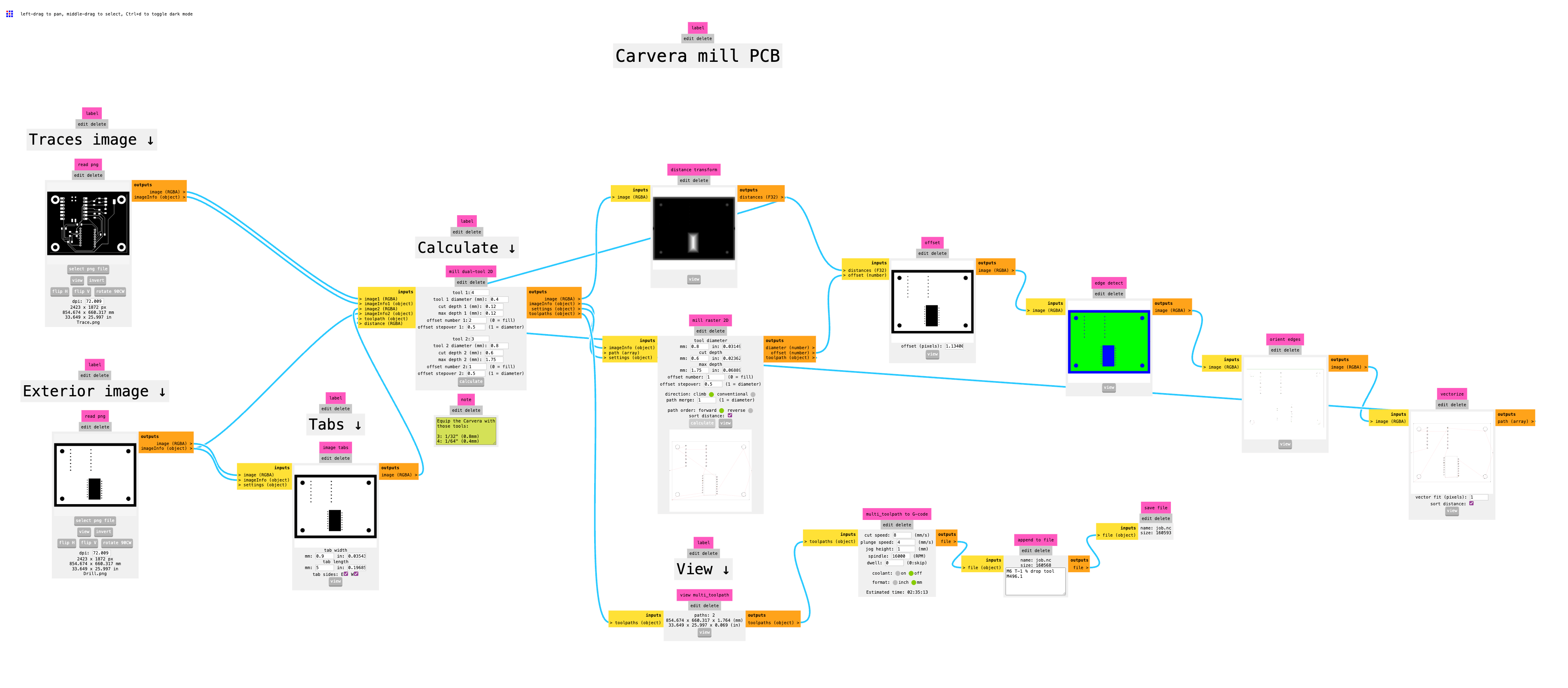
The workflow in mods:
- Right click and select
programs->open programs->Carvera - mill 2D PCB - Import the trace and exterior PNG images from gerber2img (double check if the dpi is set to 1000)
- Click
calculateunder the "Calculate ↓" section. - The toolpath preview will show up, and you will automatically download the toolpath file
job.nc
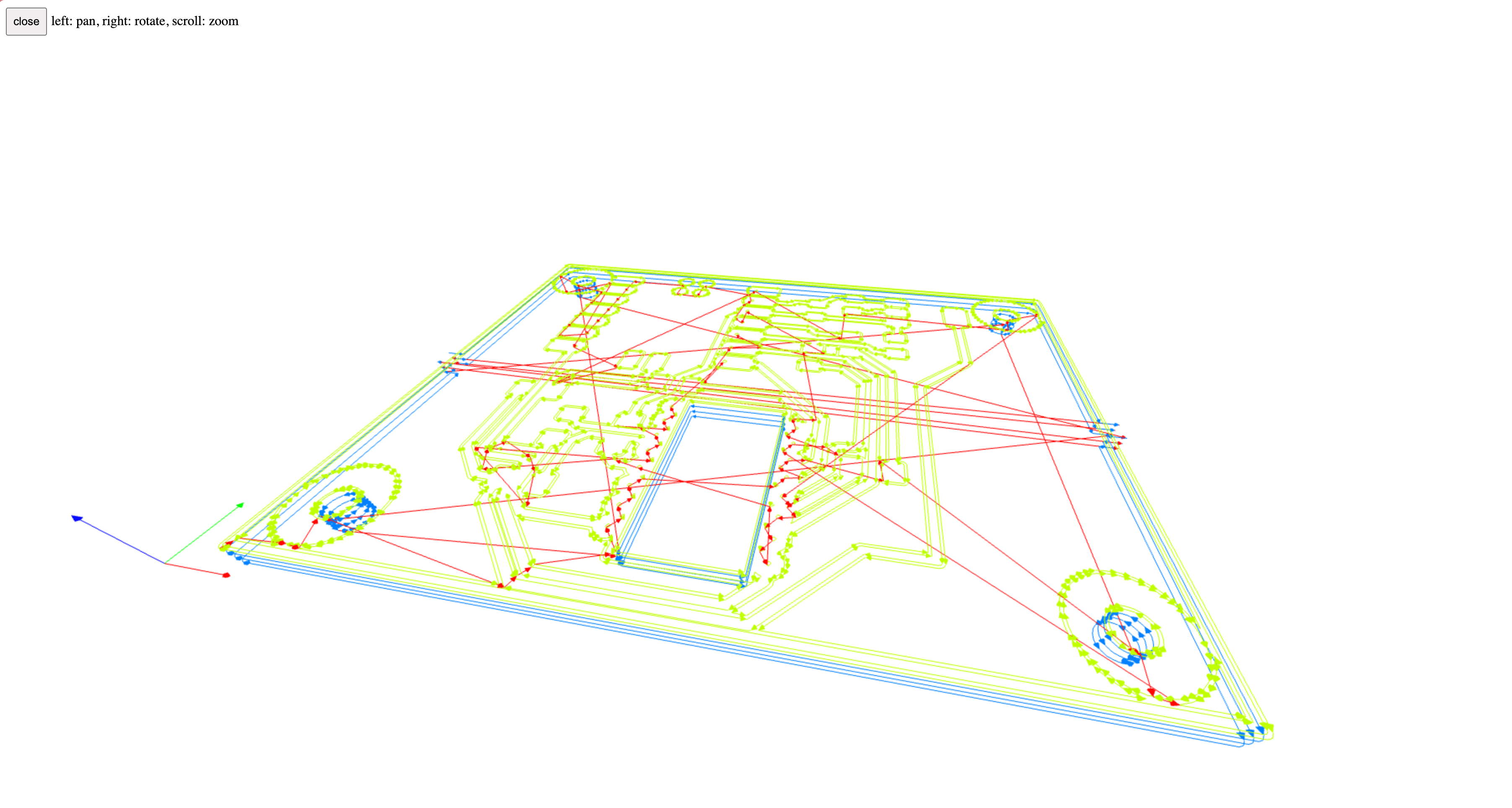
The toolpath preview looked perfect - including the drill path around the rectangular cutout I had manually added.
Milling the PCB
Time to mill! I loaded the FR-1 copper board into the Carvera and ran the toolpaths.
The milling process went smoothly:
- Trace milling: Isolated the copper traces
- Drilling: Created holes for through-hole components and vias
- Outline cut: Cut the board to size and created the rectangular cutout
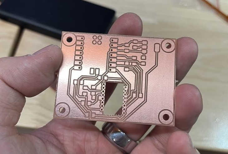
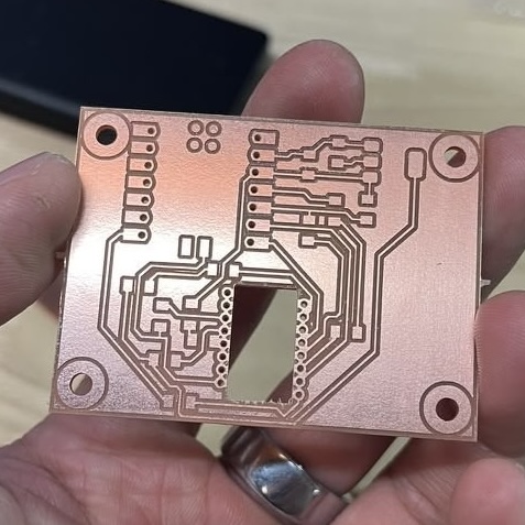
The rectangular cutout came out clean, confirming that the manual Photoshop edit worked as intended.
The only problem is that the pads for the PMW3360 sensor pins are connected to each other, so I needed to use a cutter to manually separate them before assembly.
Giving Up
By the time I had a chance to revisit this project and fix the connected pads, I had already decided that my final project wouldn't need this optical sensor as part of the design. Rather than spending more time debugging and fixing this board, I decided to put it aside for now.
The rest of the PCB fabrication assignment requirements are fulfilled in Week 12, where I designed, fabricated, and thoroughly tested another PCB board.
References
- AMS1117 Datasheet
- gerber2img Tool
- Mods Project
- SnapMagic PMW3360
- PixArt PMW3360 Datasheet
- AMS1117 Regulators on Amazon